Hdi board introduced
hdi board (
高密度内部连线)
, namely high density interconnect board, is the use of micro buried blind hole technology of a circuit board line distribution density is higher.
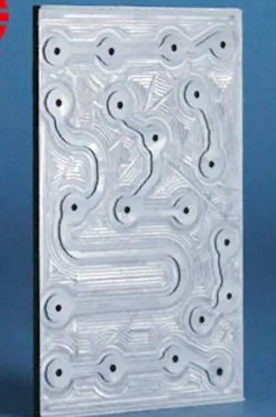
HDI board has the inner line and the outer line, using the drilling, hole metallization process, such as make each layer of internal implementation link.
HDI board general product layer method is used to manufacture, horizon, the more the higher the technical level of panel.
Ordinary HDI board is basically one horizon, high-order HDI using 2 or more horizon technology, at the same time with pile hole, electroplating fill holes, laser punching technology and other advanced PCB directly.
HDI PCB when the density of PCB increase after more than eight layer circuit boards, HDI to manufacture, the cost will be more traditional complex pressure also is low.
HDI board is conducive to the use of advanced packaging technology, its performance and accuracy of the signal is higher than the traditional PCB.
In addition, the HDI board to radio frequency interference and electromagnetic interference, electrostatic discharge, and heat conduction has a better improvement.
Electronic products to high density, high precision, the so-called 'high', in addition to improve the machine performance, but also the volume of the machine.
High density integration (
HDI)
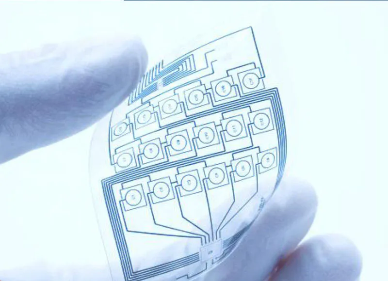
Technology can be further miniaturization of terminal product design, and satisfy the higher standards of electronic performance and efficiency.
Currently popular electronic products, such as mobile phones, digital (
Taken)
Like a machine, notebook computers, automotive electronics, etc. , many of them are using HDI board.
With the upgrading of electronic products and the demand of the market, the development of the HDI board will very quickly.
General introduce PCB PCB (
印刷电路板)
, say again in Chinese
printed circuit board, printed circuit board, is an important electronic components, electronic components to support the body, is the carrier of electronic electrical connection.
Since it is made of electronic printing, therefore is called 'printed circuit board.
Its role is mainly electronic equipment adopts the PCB, due to the consistency of the same kind of PCB, so as to avoid the artificial connection error, and can realize automatic instrumentation or SMT electronic components, automatic soldering, automatic detection, ensure the quality of the electronic equipment, improve the labor productivity, reduce the cost, and easy maintenance.
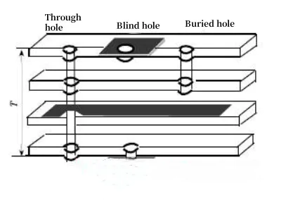
There are blind buried holes of the PCB are called hdi board?
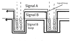
HDI PCB HDI board high-density interconnect circuit boards, blind hole plating and secondary pressure plate are HDI board, points the first-order and second-order, third-order and fourth-order, five order HDI, such as the iPhone 6 motherboard is five HDI.
Simply buried hole is not necessarily the HDI.
HDI PCB first and second order and third order how to distinguish the first-order is simpler, process and process control.
Second order began to trouble, a counterpoint, a punch and copper plating problem.
There are many types of the design of the second order, one is the order stagger position, needs to connect when adjacent layer through a conductor in the middle tier is equivalent to two first-order HDI.
The second is, two first-order holes overlap, by superimposing way to realize the second order, two first-order processing is similar, but there are many key points to control, which is mentioned above.
The third is directly from the outer punch to layer 3 (
Or N -
Layer 2)
, craft and there are many different front, the difficulty of the punch.
For the third order to second-order analogy is.
Hdi board and the difference between ordinary ordinary PCB PCB plank is FR -
Level 4, its for epoxy resin and electronic glass cloth bonding.
Conventional HDI, the outside with back glue, copper foil, because the laser drilling, unable to get through the glass cloth, so generally want to use glass fiber back glue copper foil, but now has high energy laser drill can play through 1180 glass cloth.
So no difference and common materials.
One increasingly popular managerial tactic to improve problem-solving performance of pcb making service is to increase the connectedness, or what academics call clustering, of the organization
For more tips and strategies on effective
pcb manufacturing services solutions, get your choice at Rocket PCB .
On top of making sure all our day-to-day operations are running smoothly, Rocket PCB Solution Ltd. needs to ensure that we're keeping up with all the quality standards of pcb making service.