
English


IC substrates serve as the connection between IC chip(s) and the PCB through a conductive network of traces and holes. IC substrates are endowed with critical functions including circuit support and protection, heat dissipation, and signal and power distribution.
IC substrates represent the highest level of miniaturization in PCB manufacturing and share many similarities with semiconductor manufacturing. Rocket PCB produces many types of IC substrates on which IC chips are attached to the IC substrate utilizing wire bonding or flip chip methods.
With the rapid development of BGA (ball grid array) and CSP (chip level package) and other new ICs, IC substrate has been booming, these ICs need new packaging substrate. As one of the most advanced PCB (printed circuit board), IC substrate PCB, along with any layer of HDI PCB and rigid-flex PCB, has explosive growth in popularity and application. Now it is widely used in Telecom and electronic updates.
IC substrate is a kind of substrate used to package bare IC (integrated circuit) chips. Connecting chips and circuit boards, IC is an intermediate product with the following functions:
It captures semiconductor IC chips
There are wiring connection chip and PCB inside
It can protect, strengthen and support the IC chip, providing heat tunnel
IC packaging substrate is developed on the basis of HDI / BUM board, or IC packaging substrate is HDI/ BUM board with higher density.
BGA IC substrate: The IC substrate performs well in heat dissipation and electrical performance, and can significantly increase the chip pins. Therefore, it is suitable for IC packages with more than 300 pins.
CSP IC substrate: CSP is a single chip package, lightweight, small size, with a size similar to IC. CSP IC substrate is mainly used in memory products, telecommunication products, and electronic products with a small number of pins.
FC IC substrate: FC (flip chip) is a flip-chip package with low signal interference, low circuit loss, good performance, and effective heat dissipation.
MCM IC substrate: MCM is the abbreviation of a multi-chip module. This type of IC substrate absorbs chips with different functions into a package. Therefore, due to its features including lightness, thinness, shortness, and miniaturization, the product can be the best solution. Of course, because multiple chips are packaged in one package, this type of substrate does not perform well in signal interference, heat dissipation, fine wiring, and so on.
Rigid IC substrate: It is mainly made of epoxy resin, BT resin, or ABF resin. It's CTE (coefficient of thermal expansion) is about 13 to 17ppm /℃
Flex IC substrate: It is mainly made of PI or PE resin and has CTE 13 to 27ppm / ℃·
Ceramic IC substrate: It is mainly made of ceramic materials, such as alumina, aluminum nitride, or silicon carbide. It has a relatively low CTE of about 6 to 8 ppm / ℃
Wire bonding
TAB
FC bonding
IC PCB is mainly used in lightweight, powerful electronic products, such as smartphones, laptops, tablets and networks, telecommunications, medical, industrial control, aerospace, and military fields.
The development of rigid PCB has gone through a series of innovative substrate PCBs from multilayer PCB, traditional HDI PCB, SLP (substrate-like PCB) to IC. SLP is just a rigid PCB, and its manufacturing process is similar to that of semiconductor scale.
The main application fields of IC substrate include CPU, North-South Bridge chip, graphics card chip, memory chip, communication chip, game machine chip, and so on.
IC substrate board is also a product based on BGA (ball grid array) architecture. Its manufacturing process is similar to that of PCB products, but its precision is greatly improved, and there are differences between IC substrate board and PCB in material design, equipment selection, post-process, etc. IC substrate has become a key component in IC packaging, gradually replacing some lead frame applications. Compared with standard PCB, IC substrate must overcome the difficulties of high performance and advanced function in manufacturing.
The IC substrate is thin and easy to deform, especially when the thickness is less than 0.2mm. In order to overcome this difficulty, breakthroughs must be made in plate shrinkage, lamination parameters, and layer positioning system, so as to effectively control substrate warpage and lamination thickness.
Microvia technology includes the following aspects: conformal mask, laser drilling micro blind through-hole technology, and copper plating filling technology.
The purpose of the conformal mask is to logically compensate the laser drilling through the opening, and the blind hole can be directly located through the aperture.
Laser drilling micromachining is related to the following technologies: through-hole shape, aspect ratio, side etching.
Blind hole copper coating with the following technical aspects: through-hole filling ability, blind hole opening, sinking, copper plating reliability, etc.
Patterning and copper plating technology are related to the following technical aspects: circuit compensation technology and control, thin wire manufacturing technology, copper plating thickness uniformity control.
The fabrication of IC PCB solder masks includes through-hole filling technology, solder mask printing technology, and so on. So far, the surface height difference of IC PCB is less than 10um, and the surface height difference between solder mask and pad should not exceed 15 microns.
The thickness uniformity should be emphasized in the surface treatment of IC PCB. Up to now, the acceptable surface treatment of IC PCB includes ENIG / ENEPIG.
IC PCB requires different testing equipment from traditional PCB. In addition, there must be engineers who can master the testing skills of special equipment.
In a word, IC substrate PCB requires more requirements than standard PCB and HDI PCB. Manufacturers must have advanced manufacturing capabilities and be proficient in them.
The most important feature of IC substrate structure is micro through hole
These customers can be divided into two categories, the first category is PC, communication, game machine chip factory, including
1. CPU class: Intel, AMD;
2. North-South Bridge: via (Weisheng), SIS;
3. Graphics: NVIDIA, ATI;
4. Storage: Samsung, Toshiba, Xindi, Marvell, etc;
5. Communication: Broadcom, Motorola, Marvell;
6. Other semiconductor companies: Altera, Xilinx, STM, etc.
The second category is packaging and testing plants, such as silicon products, Sunmoon and Amkor. Among them, silicon products and Sunmoon are the top two packaging and testing plants in Taiwan, China, and Amkor is the world's largest packaging and testing plant.
Application fields and main customers distribution of IC substrate factory
IC substrate factory | Application fields | Main customers |
Nanya | CPU, North-South Bridge chip | Intel、nVidia、Broadcom
|
Quan Mao | Graphics card, North-South Bridge chip, mobile phone chip | ATI, NVIDIA, via, SIS, Broadcom, silicon products |
KINSUS | Graphics card, North South Bridge chip, network, DSP | ATI, NVIDIA, Altera, Xilinx, Amkor, Marvell, Xindi, silicon products, Sunmoon
|
Unimicron | Flash memory card, digital camera chip, wireless network chip | Motorola、STM、Amkor |
Riyuehong | Graphics card, North-South Bridge chip | ase |
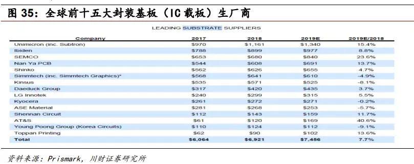
At present, the global packaging substrate market is basically occupied by the PCB enterprises in Taiwan of China such as UMTC, IBEDEN, SEMCO, NANYA, KINSUS, and other countries, as well as Japan and South Korea. The market share of the top ten enterprises is more than 80%, and the industry concentration is high.
At present, the world's main production bases are in Japan, Taiwan, and South Korea. The main manufacturers include Japan's Yifei electric, Shengang electric, Kyocera, Eastern, South Korea's Samsung electric, LG Innotek, Xintai electronics, Daeduke, KCC, and Taiwan's Unimicron Electronics, KINSUS, NAN YA, And ASE.
At present, the mainstream products of domestic production are FC CSP, FC BGA, and WB BGA / CSP. It is expected that FC CSP will maintain rapid growth in the next few years. In the domestic market, IC packaging substrates are mainly used in smartphones, tablet computers, PCs, communication devices, and storage. In the future, with the transformation and upgrading of China's manufacturing industry, the strategic importance of the semiconductor industry is becoming increasingly prominent, the establishment of the concept of green development, and the rapid development of the Internet of things, new energy vehicles, and other emerging industries in China, the rapid development of China's semiconductor industry will be driven, Further drive domestic IC packaging substrate production and demand.
Top 15 packaging substrate (IC substrate) manufacturers in the world
However, as the PCB industry in the United States, Japan, South Korea, Taiwan, and other regions has entered a mature or even recession period, its output value is also gradually showing a downward trend. Chuan Cai Securities pointed out in the research report that Japan, which represents the global high-end PCB manufacturing level and guides the global PCB development direction, has weakened its competitiveness in recent years due to its market strategy and price level.
China's local PCB enterprises are expected to share the dividend of industrial transfer and industry concentration and are gradually undertaking the PCB production capacity of other countries and regions. With the significant increase of capacity utilization rate of SMIC international and Huahong semiconductor's domestic two major generation factories, it will drive the development of its downstream packaging and testing manufacturers.
In the field of conventional packaging substrate, the products of domestic manufacturers such as Shennan circuit, FastPrint Technology, and Zhuhai ACCESS have been mass-produced, and the technology is relatively mature, and they have successively announced the expansion of production. Industry insiders believe that with the gradual expansion of the scale of domestic substrate manufacturers, the follow-up cost advantage will be obvious.
In addition, domestic manufacturers speed up the layout of HDI products and catch up with Taiwan manufacturers. The production capacity is concentrated in the second half of 2021, and the HDI mainly launched is still in short supply for the high-end production capacity of first-order, second-order, third-order, and any layer.
QUICK LINKS
CONTACT US
Office: (+86) 755 23040566
Tel: (+86) 158 9965 5195
E-mail: sales@rocket-pcb.com
Skype: Hans@Rocket-PCB
Whatsapp: 86 1589965 5195
Office Address: 2207,Bid 4,He Gu Shan Hui Cheng,35#,Guang Tian RoYanluo street, Song Gang Town,518105 SHENZHENG, CHINA
Plant ADD.: No 69, Lianfeng North Road, Xianxi Area, ChangAn Town, Dongguan, China.


