


IC substrate technology Guide
What is IC substrate?
IC substrate (also known as IC package substrate) is a key special basic material used in advanced packaging, which is used to package bare IC (integrated circuit) chips. IC substrate acts as the connection between IC chip and PCB through a conductive network of wires and holes. IC packaging substrate is developed on the basis of HDI / BUM board, or IC packaging substrate is HDI / BUM board with higher density.
IC is an intermediate product, which has the following functions:
Capture semiconductor IC chip;
Internal wiring for connecting chip and PCB;
It can protect, reinforce and support IC chips, and provide a heat dissipation channel
Signal and power distribution
Advanced technology IC substrates include:
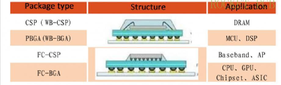
CSP (Chip Scale Packages)
FC-CSP (Flip Chip) CSP
BOC (Board on Chip)
PoP (Package on Package)
PiP (Package in Package)
SiP (System in Package)
RF Module
LED Package
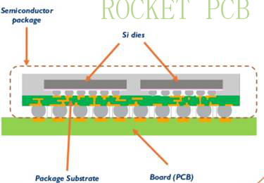
IC substrates serve as the connection between IC chip(s) and the PCB through a conductive network of traces and holes. IC substrates are endowed with critical functions including circuit support and protection, heat dissipation, and signal and power distribution.
IC substrates represent the highest level of miniaturization in PCB manufacturing and share many similarities with semiconductor manufacturing. Rocket PCB produces many types of IC substrates on which IC chips are attached to the IC substrate utilizing wire bonding or flip-chip methods.
With the rapid development of BGA (ball grid array) and CSP (chip level package) and other new ICs, IC substrate has been booming, these ICs need new packaging substrate. As one of the most advanced PCB (printed circuit board), IC substrate PCB, along with any layer of HDI PCB and flexible rigid PCB, has explosive growth in popularity and application. Now it is widely used in Telecom and electronic updates.
The birth of IC substrate
Traditional integrated circuit (IC) packaging uses a lead frame as the substrate of IC conduction line and supporting IC, connecting pins on both sides or around the lead frame, such as a two-sided pin flat package, four side pin flat package, and so on. When the number of pins is not too much, this packaging method can also meet the requirements. With the development of semiconductor technology, the characteristic size of IC is shrinking and the integration degree is improving. The corresponding IC package is developing towards the direction of ultra multi-pin, narrow pitch, and ultra miniaturization. The traditional lead package has been unable to meet the requirements. In the 1990s, a ball grid array (BGA), chip-scale package (CSP), and other new IC high-density packaging methods began to appear, so an IC substrate PCB emerged.
Classification of IC substrate
As mentioned above, there are many ways to classify packaging substrates, mainly by packaging process, material properties, and application fields.
1. According to the packaging processes
packaging substrate can be divided into wire bonding packaging substrate and the flip-chip packaging substrate.
1.1 Classification by bonding technology
Wire bonding
TAB
FC bonding
1.2 flip-chip packaging substrate
BGA IC substrate: The IC substrate performs well in heat dissipation and electrical performance, and can significantly increase the chip pins. Therefore, it is suitable for IC packages with more than 300 pins.
CSP IC substrate: CSP is a single chip package, lightweight, small size, with a size similar to IC. CSP IC substrate is mainly used in memory products, telecommunication products, and electronic products with a small number of pins.
FC IC substrate: FC (flip chip) is a flip-chip package with low signal interference, low circuit loss, good performance, and effective heat dissipation.
MCM IC substrate: MCM is the abbreviation of a multi-chip module. This type of IC substrate absorbs chips with different functions into a package. Therefore, due to its features including lightness, thinness, shortness, and miniaturization, the product can be the best solution. Of course, because multiple chips are packaged in one package, this type of substrate does not perform well in signal interference, heat dissipation, fine wiring, and so on.
2. According to different substrate materials
Packaging substrate can be divided into the rigid board, flex board, and ceramic substrate.
Rigid IC substrate: It is mainly made of epoxy resin, BT resin, or ABF resin. Its CTE (coefficient of thermal expansion) is about 13 to 17ppm /℃
Flex IC substrate: It is mainly made of PI or PE resin and has CTE 13 to 27ppm / ℃·
Ceramic IC substrate: It is mainly made of ceramic materials, such as alumina, aluminum nitride, or silicon carbide. It has a relatively low CTE of about 6 to 8 ppm / ℃
3. According to different application fields
Packaging substrates can be divided into memory chip packaging substrates, MEMS packaging substrates, RF module packaging substrates, processor chip packaging substrates, and high-speed communication packaging substrates, which are mainly used in mobile intelligent terminals, services/storage, etc.
Manufacturing technology of IC substrate
First of all, we need to understand three kinds of PCB manufacturing processes. At present, there are three kinds of PCB and IC substrate manufacturing processes, namely, subtractive process (SP), additive process (AP), and modified semi-additive process (MSAP).
1. Subtraction method (SP): the most traditional PCB manufacturing process, first plating a certain thickness of a copper layer on the copper-clad laminate, and then using a dry film to protect the circuit and through-hole, and etching the unnecessary copper sheet. The biggest problem of this method is that during the etching process, the side of the copper layer will also be etched. Due to the existence of lateral etching, the minimum line width/spacing of PCB can only be greater than 50 μ m (2mil), so it can only be used in ordinary PCB, FPC, and HDI PCB products.
2. Addition method (AP): firstly, the circuit is exposed to the insulating substrate containing photosensitive catalyst, and then selective chemical copper deposition is carried out on the exposed thick circuit to obtain a complete PCB. This method does not need lateral etching, so it can achieve very high accuracy, and the fabrication can reach less than 20 μm. At present, this method has high requirements for substrate and process flow, high cost, and low output; it is mainly used to produce WB or FC IC substrate, and its process can reach 12 μ M / 12 μ M.
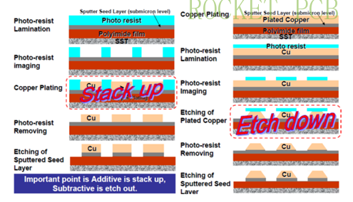
Addition vs. subtraction
3. Modified semi-additive process (MSAP): firstly, the thin copper layer is electroplated on the copper-clad laminate, then the areas that do not need to be electroplated are protected, and then electroplated again and coated with anti-corrosion coating, and then the more chemical copper layer is removed by flash etching, leaving the required copper layer line. Because the copper layer is very thin at the beginning of electroplating, the time of flash corrosion is very short, so the side corrosion has a small influence.
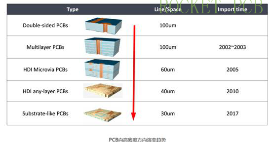
Compared with the subtraction method and addition method, the MSAP process has the advantages of high yield and low production cost, which is the most popular manufacturing method of the fine circuit board. This technology is widely used in the manufacturing of CSP, WB, and FC IC substrate and other fine line substrate boards. Although the SLP (substrate-like PCB) belongs to the printed circuit board, its minimum line width/line spacing is 30 μ M / 30 μ m from the process point of view, so it can not be produced by subtraction method, and MSAP process technology is also needed.
Industry barriers of IC substrate
IC substrate board is developed from HDI board, and there is a certain correlation between them, but the technical threshold of IC substrate board is much higher than HDI and ordinary PCB. IC substrate board can be understood as a high-end PCB, which has the characteristics of high density, high precision, high pin count, high performance, miniaturization, and thinness. It has higher requirements in a variety of technical parameters, especially the core line width/line distance parameter. Take the chip packaging substrate of mobile product processor as an example, it's line width/line spacing is 20 μ M / 20 μ m, and it will continue to reduce to 15 μ M / 15 μ m, 10 μ M / 10 μ m in the next 2-3 years, while the general PCB line width/line spacing is more than 50 μ M / 50 μ M.
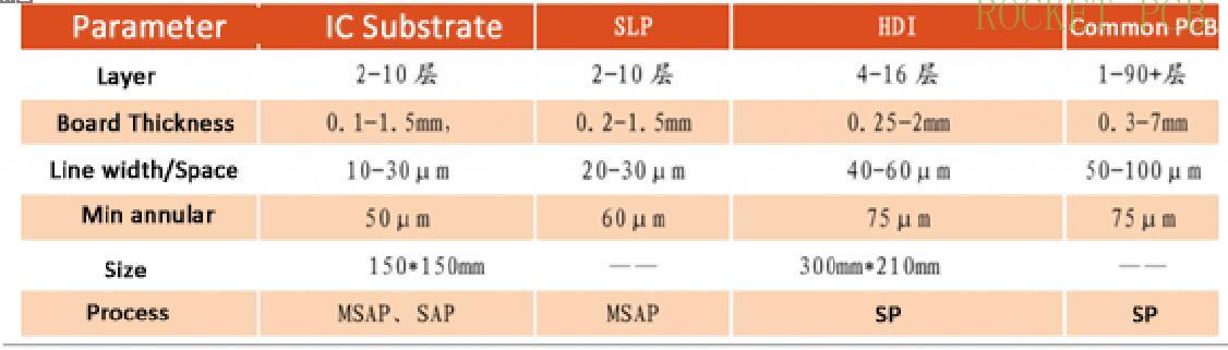
Comparison of technical parameters of IC substrate board, SLP, HDI, and ordinary PCB
Technical barriers of IC substrate
Compared with ordinary PCB, there are many technical difficulties in the IC substrate board. These technical difficulties are the biggest industry access threshold of IC substrate board. The following summarizes several technical difficulties of the IC substrate board.
Manufacturing difficulties of IC substrate PCB
Ultrafine UV laser drilling blind hole
IC substrate board is also a product based on BGA (ball grid array) architecture. Its manufacturing process is similar to that of PCB products, but its precision is greatly improved, and there are differences between IC substrate board and PCB in material design, equipment selection, post-process, etc. IC substrate has become a key component in IC packaging, gradually replacing some lead frame applications. Compared with standard PCB, IC substrate must overcome the difficulties of high performance and advanced function in manufacturing.
a. substrate manufacturing
The IC substrate is thin and easy to deform, especially when the thickness is less than 0.2mm. In order to overcome this difficulty, breakthroughs must be made in plate shrinkage, lamination parameters, and layer positioning system, so as to effectively control substrate warpage and lamination thickness.
b. Microvia manufacturing technology
Microvia technology includes the following aspects: conformal mask, laser drilling micro blind through-hole technology, and copper plating filling technology.
The purpose of the conformal mask is to logically compensate the laser drilling through the opening, and the blind hole can be directly located through the aperture.
Laser drilling micromachining is related to the following technologies: through-hole shape, aspect ratio, lateral etching.
Blind hole copper coating with the following technical aspects: through-hole filling ability, blind hole opening, sinking, copper plating reliability, etc.
c. Patterning and copper plating technology
Patterning and copper plating technology are related to the following technical aspects: circuit compensation technology and control, thin wire manufacturing technology, copper plating thickness uniformity control.
d. Solder mask
The fabrication of IC PCB solder masks includes through-hole filling technology, solder mask printing technology, and so on. So far, the surface height difference of IC PCB is less than 10um, and the surface height difference between solder mask and pad should not exceed 15 microns.
e. Surface treatment
The thickness uniformity should be emphasized in the surface treatment of IC PCB. Up to now, the acceptable surface treatment of IC PCB includes ENIG / ENEPIG.
f. Testing capability and product reliability testing technology.
IC PCB requires different testing equipment from traditional PCB. In addition, there must be engineers who can master the testing skills of special equipment.
In a word, IC substrate PCB requires more requirements than standard PCB and HDI PCB. Manufacturers must have advanced manufacturing capabilities and be proficient in them.
The most important feature of IC substrate structure is micro through hole
IC substrate production process is complex, and the MSAP process is the mainstream. The minimum line width/spacing of IC substrate is generally less than 30 μ M. the traditional subtraction process has been difficult to meet the requirements of IC substrate. MSAP is the most common process for IC substrate manufacturing. In addition to being widely used in IC substrate manufacturing, MSAP technology is also introduced into SLP (substrate-like) manufacturing by apple. The current design is to use a mixture of reduced etching and MSAP process, MSAP process can be applied to thinner, smaller motherboard design.
The barriers of the IC substrate industry are high, not limited to the technical threshold. High technical requirements and numerous patent restrictions have created a high threshold of the IC substrate industry, and the barriers of the industry also include capital and customers.
Capital Barrier of IC substrate
Due to the high technical barriers of the IC substrate board, the initial R & D investment is huge and time-consuming, and the development risk of the project is high. The construction and subsequent operation of the IC substrate board production line also need huge capital investment, among which the capital investment of equipment is the largest. There are many devices in the IC substrate production line, and the price of a single device may exceed 10 million yuan. The equipment/instrument investment accounts for more than 60% of the total investment of the IC substrate projects, which is a heavy burden for traditional PCB manufacturers. Taking Fast Print technology as an example, the company launched the IC substrate project in 2012, with a total investment of more than 400 million yuan. It is estimated that the project will reach its production capacity in three years, and the annual output value will be about 500 million yuan after it reaches its production capacity. However, the company's IC substrate project is difficult to carry out in the early stage, with a loss of more than 400 million yuan over the years, which seriously hinders the company’s performance. It will gradually improve in 2018 six years later.
Customer barriers of IC substrate
IC substrate customer verification system is more strict than PCB, which is related to the quality of chip and PCB connection. The industry generally adopts the "qualified supplier certification system", which requires suppliers to have a sound operation network, efficient information management system, rich industry experience, and good brand reputation, and need to pass strict certification procedures. The certification process is complex and the cycle is long. Take Fast Print technology as an example. After nearly two years of verification and cooperation, the company passed Samsung certification in September 2018, and it will take some time to supply Samsung with large-scale products.
Environmental protection barrier of IC substrate board
Similar to PCB, the manufacturing process of IC substrate involves a variety of chemical and electrochemical reactions, and the production materials also contain heavy metals such as copper, nickel, gold, silver, which have certain environmental risks. With the increasing attention of the state to environmental protection and the continuous introduction of environmental protection policies, the preliminary environmental impact assessment of IC substrate projects is becoming more and more difficult, and the stricter environmental protection also further improves the industry’s capital threshold, and it is difficult for enterprises with insufficient capital strength to get industry access tickets.
The supply chain of IC substrate
IC Packaging substrate is the largest cost of IC packaging, accounting for more than 30%. The cost of IC packaging includes packaging substrate, packaging materials, equipment depreciation, and testing. The cost of IC substrate board accounts for more than 30% of the total cost of IC packaging, which plays an important role in IC packaging. For IC substrates, the substrate materials include copper foil, substrate, dry film (solid photoresist), wet film (liquid photoresist), and metal materials (copper ball, nickel bead, and gold salt). The substrate accounts for more than 30%, which is the largest cost side of IC substrates.

Composition of IC packaging cost
One of the main raw materials: copper foil
Similar to PCB, the copper foil for IC substrate board is also electrolytic copper foil, and it needs to be an ultra-thin uniform copper foil, with the minimum thickness of 1. 5 μ m, generally, 9-25 μ m, while the thickness of copper foil for traditional PCB is about 18 and 35 μ M. The price of ultra-thin uniform copper foil is higher than that of ordinary electrolytic copper foil, and the processing difficulty is also greater.
The second main raw material: substrate
The substrate of the IC substrate board is similar to the copper-clad laminate of PCB, which is mainly divided into the hard substrate, flexible film substrate, and co-fired ceramic substrate. The hard substrate and flexible substrate have more development space, while the co-fired ceramic substrate tends to slow down. The main factors of IC substrate include dimensional stability, high-frequency characteristics, heat resistance, and thermal conductivity. At present, there are three kinds of hard packaging substrate materials, namely BT material, ABF material, and MIS material; flexible packaging substrate materials mainly include PI (polyimide) and PE (polyester) resin; ceramic packaging substrate materials mainly include alumina and nitriding Aluminum, silicon carbide and other ceramic materials.
Substrate classification | Substrate material | Brief introduction | Main application fields |
Hard substrate | BT | BT resin has many advantages such as high Tg, high heat resistance, moisture resistance, low dielectric constant (DK) and low loss factor (DF), but it can not meet the requirements of thin line | MEMS, communication and memory chips, and LED chips |
ABF | Led by Intel, it can be used as IC with thin circuit, high pin number and high transmission, and has great development potential in the future | It is mainly used for large high-end chips such as CPU, GPU and chipset | |
MIS | Different from the traditional substrate, it contains one or more layers of pre encapsulated structure, each layer is interconnected by electroplating copper to provide electrical connection in the packaging process | It has developed rapidly in analog, power IC and digital currency markets | |
Flexible substrate | PI | It is mainly divided into three-layer glued substrate and two-layer non glued substrate, with excellent heat resistance, good moisture absorption and mechanical properties | It can be used in carrier rocket, cruise missile, space satellite and other military chips, as well as automotive electronics, consumer electronics and other chips |
PE | |||
Ceramic substrate | Alumina | Ceramics are inorganic insulating materials, which have the advantages of heat resistance, thermal stability and high-frequency characteristics, but the machinability is poor and the cost is high | It is mainly used in thick film circuit, thin-film circuit and military chip |
Aluminum nitride | |||
Silicon carbide |
Material classification of the packaging substrate
There are many manufacturers of upstream substrate materials, and the domestic technology is relatively weak. There are many kinds of IC substrate core materials, and most of the upstream manufacturers are foreign-funded enterprises. Take the largest BT materials and ABF materials, for example, the main manufacturers of BT resins are Japanese Mitsubishi Gas Chemical and Hitachi chemical products. China is mainly in the Taiwan area with a large capacity, including Kin sua, Unimicron, and South power. There are few mainland enterprises. ABF materials include South power, Ibiden, Shinko, Semco, etc., Unimicron is actively catching up with the progress, and domestic enterprises in mainland China are rarely involved. As far as Chinese enterprises are concerned, Shengyi technology is in the forefront of R & D and the production of IC substrate. In May 2018, the company announced that the "annual production of 17 million square meters of copper-clad laminate and 22 million meters of commercial adhesive sheet construction project" will be changed, and the original project implementation site will be planned to build a production line of substrate materials for packaging substrate plate. The company’s layout at the substrate end of IC substrate board is expected to break through the technical encirclement of foreign giants and accelerate the domestic substitution process of the PCB and IC substrate board.
IC substrate is widely used in many fields. Mainstream packaging substrate products are roughly divided into five categories, namely, memory chip packaging substrate, MEMS packaging substrate, RF module packaging substrate, processor chip packaging substrate, and the high-speed communication packaging substrate. These chips have basically adopted a substrate packaging scheme due to their high integration. With the continuous improvement of IC integration, the proportion of other chips using IC substrate will also increase.
Application of IC PCB
IC PCB is mainly used in lightweight, powerful electronic products, such as smartphones, laptops, tablets and networks, telecommunications, medical, industrial control, aerospace, and military fields.
The development of rigid PCB has gone through a series of innovative substrate PCBs from multilayer PCB, traditional HDI PCB, SLP (substrate-like PCB) to IC. SLP is just a rigid PCB, and its manufacturing process is similar to that of semiconductor scale.
The main application fields of IC substrate include CPU, North-South Bridge chip, graphics card chip, memory chip, communication chip, game machine chip, and so on.
IC substrate from Rocket PCB
Rocket PCB can fabricate IC substrate for flip-chip packaging. The substrate has a variety of single-chip and multi-chip, BGA, and LGA dimensions. It can be used for high I / O, high-performance applications, and has micro bumps for C4 or TCB chip attachment. The substrate may have surface-mounted passive components on one or both sides and be delivered as a single Fab in an array bar or JEDEC tray. Our advanced construction process, highly automated, contactless and fully contained in the cleanroom, first forms reinforced core plates with filled cores or copper-filled buried holes, thus providing a platform for copper circuits formed by multi-layer alternating stacking of unreinforced dielectric films via semi addition process (SAP). This multifunctional system provides the best balance between performance, reliability and value for industry-leading high-density interconnection products.
Related Post
Overview of global IC substrate enterprises in 2021


