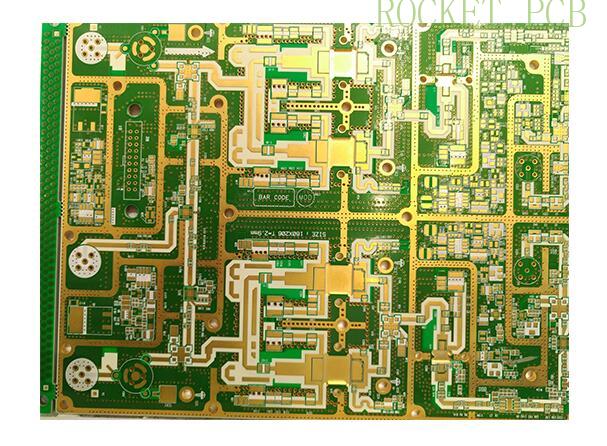
Advanced PCB Fabrication: Techniques and Trends to Watch
Introduction
PCB (Printed Circuit Board) fabrication designs and manufactures the physical board that supports and connects electronic components. It involves the creation of a conductive pathway etched onto the board, which allows for the transfer of electrical signals between components.

Why is PCB fabrication essential?
PCB fabrication is a critical component of the electronics industry, as it is the foundation for creating a wide range of electronic devices. It is a complex and precise process that requires skilled professionals and specialized equipment.
In this article, we will explore advanced PCB fabrication techniques and trends that are shaping the industry. We will discuss the benefits and drawbacks of each method, as well as the challenges and opportunities presented by emerging trends. We will also answer common questions that users may have about PCB fabrication.
With this knowledge, readers will be better equipped to understand and navigate the PCB fabrication process and to make informed decisions about their projects. Let's begin by examining some of the advanced PCB fabrication techniques.
Advanced PCB Fabrication Techniques
Traditional PCB fabrication methods
Traditional PCB fabrication methods have been used for decades and include etching, drilling, and soldering. These methods are still widely used in the industry, but they have limitations in terms of precision and speed.
Introduction to advanced techniques
Advanced PCB fabrication techniques have emerged in recent years that offer greater precision, speed, and efficiency. Laser Direct Imaging (LDI), Plating Over Via (PoV), and Microvia Drilling are three techniques.
Laser Direct Imaging (LDI)
LDI is a process that uses a laser beam to create a high-resolution image on a photosensitive material. This image is then used to generate the circuit pattern on the board, eliminating the need for a traditional photomask. LDI provides high accuracy and speed, making it ideal for high-volume production.
Plating Over Via (PoV)
PoV is a technique that involves adding a thin layer of copper over the vias on the board, which are the holes that connect different layers. This process helps to reduce the size of the vias, which improves the density of the board and allows for smaller and more complex designs.
Microvia Drilling
Microvia drilling is a process that uses lasers to drill small holes in the board. These holes are then plated with copper, connecting different board layers. Microvia drilling allows for the creation of high-density panels with many connections.
Benefits and drawbacks of each technique
Each advanced PCB fabrication technique has its own set of benefits and drawbacks. LDI provides high accuracy and speed, but it requires specialized equipment and may not be suitable for small-scale production. PoV allows for smaller vias and more complex designs but can be expensive and require additional processing steps. Microvia drilling provides high-density boards, but it can be challenging to ensure uniform plating and may require further testing.
How these advanced techniques are changing the PCB fabrication industry
Advanced PCB fabrication techniques are changing the industry by providing greater precision, speed, and efficiency. They allow for creating smaller and more complex designs, driving innovation in the electronics industry. However, these techniques require specialized equipment and expertise, making them expensive and challenging to implement for some manufacturers. As the industry continues to evolve, it will be necessary for manufacturers to stay up-to-date with the latest advances in PCB fabrication techniques to remain competitive.
PCB Fabrication Trends to Watch
emerging trends in PCB fabrication
PCB fabrication is a rapidly evolving field, and several emerging trends will likely shape its future. Some of these trends include:
1. 3D Printing: 3D printing is a technique that allows for creation of three-dimensional objects from a digital model. This technology is being applied to the design of PCBs, which could revolutionize how PCBs are manufactured.
2. Flexible PCBs: Flexible PCBs are boards that bend and flex without breaking. This technology is used in various applications, including wearable devices, medical equipment, and automotive electronics.
3. High-Frequency PCBs: High-frequency PCBs are boards designed to operate above 1 GHz. These boards are used in applications such as 5G networks, satellite communications, and radar systems.
The benefits and challenges of these trends
Each of these trends offers unique benefits and challenges. 3D printing can reduce manufacturing costs and improve design flexibility but may require significant investment in new equipment and materials. Flexible PCBs can enable new applications and improve durability, but they can also be more challenging to manufacture and test. High-frequency PCBs can enhance performance in high-speed applications but require specialized design and manufacturing techniques.
How these trends are likely to impact the PCB fabrication industry in the future
The emergence of these trends is likely to impact the PCB fabrication industry in the future significantly. 3D printing has the potential to disrupt traditional manufacturing methods, allowing for the creation of complex geometries and reducing lead times. Flexible PCBs will likely become more prevalent in various applications, including IoT devices, robotics, and aerospace. High-frequency PCBs will continue to be in demand for high-speed applications, and developing new materials and manufacturing techniques will be essential to meet this demand.
Overall, the PCB fabrication industry is undergoing rapid change, driven by technological advances and changing customer needs. Manufacturers that stay ahead of these trends and invest in new technologies and processes will likely be well-positioned to succeed in this dynamic industry.
Common PCB Fabrication Questions
You may have several questions about the process if you're new to PCB fabrication. Below are answers to some of the users' most common questions about PCB fabrication.
1.What is the minimum line width and spacing for PCB fabrication?
The minimum line width and spacing for PCB fabrication depend on the capabilities of the manufacturer and the intended use of the PCB. Generally, the minimum line width and spacing are around 0.1mm, but some manufacturers may be able to produce lines as small as 0.05mm.
2.What materials are commonly used in PCB fabrication?
The most widely used materials in PCB fabrication include copper for the conductive traces, FR4 for the substrate, and solder masks for protection. Other materials may be used depending on the specific requirements of the PCB, such as aluminum or ceramic, for high-power applications.
3.How can I ensure the reliability of my PCB design?
To ensure the reliability of your PCB design, you should follow best practices for layout and design, such as minimizing the length of traces and avoiding sharp bends. You should also conduct thorough testing and validation of your design before production to identify and address any potential issues.
4.What factors affect the cost of PCB fabrication?
Several factors can affect the cost of PCB fabrication, including the size and complexity of the board, the number of layers, the materials used, and the quantity ordered. Ordering in bulk often reduces the cost per board, and choosing standard sizes and shapes helps keep costs down.
Overall, PCB fabrication can be complex, but understanding the basics and working with a reputable manufacturer can help ensure a successful outcome.
conclusion
Staying Up-to-Date with Advanced PCB Fabrication Techniques and Trends
Printed circuit boards (PCBs) are essential in modern electronics, used in everything from smartphones and laptops to industrial machinery and medical devices. With rapid technological advancements, it is crucial to stay up-to-date with advanced PCB fabrication techniques and trends to ensure that the products produced are of the highest quality and functionality.
In this article, we discussed the importance of using advanced PCB fabrication techniques and staying up-to-date with the latest trends in the industry. We highlighted the benefits of using high-density interconnect (HDI) PCBs, flexible PCBs, and multilayer PCBs, which offer increased functionality, reduced size, and improved performance.
We also discussed the importance of selecting suitable materials for PCB fabrication, including using specialized materials such as Teflon and FR-4, to ensure that the PCBs can withstand harsh operating conditions and environmental factors.
PCB fabrication is constantly evolving, and staying up-to-date with the latest techniques and trends is crucial to remain competitive in the market. Failure to do so may produce inferior-quality products that do not meet customer expectations.
One company that has recognized the importance of staying up-to-date with advanced PCB fabrication techniques and trends is Rocket. Rocket is a leading manufacturer of high-quality PCBs in various industries, including communication, medical, military, security, industrial, and automotive.
Rocket's main products cover various PCB types, including high-speed server boards, large data memory circuit boards, high-frequency hybrid boards, multi-stage HDI boards, IOT modules, security circuit boards, and more. These products are sold globally, with a strong presence in North America, Europe, Asia Pacific, and other international regions.


