Technology in heavy copper PCB processing
For high-power, high current server power supply board and other PCB increasing demand, and these power boards need high heat resistance, high heat dissipation and other characteristics, prefer to design as heavy copper PCB. heavy copper PCB fabrication puts forward higher technical requirements for the PCB factory, which is the embodiment of the experience and PCB technology.
Due to the thick copper (≥ 3oz) characteristics of thick copper PCB, there are many processing difficulties in the PCB production, especially in the lamination process, the traditional production method, after the large copper-free area is laminated, it is easy to have the problems of the cavity and uneven thickness, which has great limitations on graphic design, PP selection, matching of lamination program, temperature rise and vacuum capacity of the laminator, the solution of the inner layer glue (flow glue route), residual copper rate control, withstand voltage requirements, the main points of thick copper PCB engineering, the treatment of circuit coils, multiple electroplating, multiple solder masks, etc. are all experience accumulation.
Rocket PCB provides prototyping and processing services for thick copper PCB, which has overcome many technical difficulties in the field of thick copper PCB production and created a perfect thick copper PCB prototyping and mass production scheme.
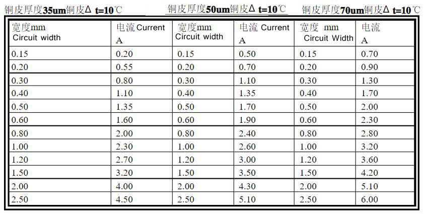
The current strength of the signal
When the average current of the signal is large, the current that can be carried by the wiring width should be considered. The line width can refer to the following data: the thickness of copper foil in PCB design, the relationship between wiring width and current, the current carrying capacity of copper foil with different thicknesses and width is shown in the table below:
The current carrying capacity of copper foil with different thicknesses and circuit width
Thick copper printed circuit board is made of thick copper foil and super thick copper foil. It uses conductive materials (copper foil) and substrate materials, production technology, application fields are different from conventional PCB, so it belongs to special PCB. Most of the thick copper printed circuit boards are high-current substrates.

Heavy copper PCB Application
The main application fields of the high current substrate are power modules and automotive electronic components. Some of its main terminal electronic product fields are the same as conventional PCB (such as portable electronic products, network products, base station equipment, etc. ), and some are different from conventional PCB fields, such as automobile, industrial control, power module, etc.
How to realize copper thickness of heavy copper circuit board?
Generally, the copper thickness of the finished product of 2oz, the silk screen printing by hand is not enough to fill the gullies between the lines, so the solder mask must be printed twice.
Therefore, in the circuit board production generally encounter 2oz and thicker will be remarked: thick copper board, need twice solder mask. In order to achieve the effect that the line does not turn red and the thickness of the solder mask on the line surface is greater than 10um.
It’s not really the thicker the hole copper is, the better. All the data need to be made according to the customer's requirements.
Copper plating usually includes primary copper and secondary copper. The main purpose of primary copper is to provide sufficient copper thickness for secondary copper etching, so as to ensure that the copper thickness after secondary copper etching can meet the customer’s standard requirements.
A thick copper circuit board can generally process 6oz, 3oz thick copper board, generally need multi-layer screen printing and multi-layer solder mask and multi-layer copper deposition to meet customer needs.
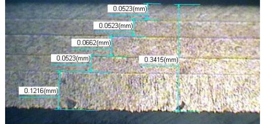
10 oz thick copper circuit metallographic section (secondary dry film method by LDI, 4 times plating)
Heavy copper PCB has the following technical points

1. Fabrication of thick copper circuit with inner and outer layers
2. The lamination of thick copper circuit core board includes resin filling of laminated circuit and control of overall board thickness
3. Influence of thick copper core board on drilling method of laminated board
4. Surface solder mask of thick copper circuit
Key points of production capacity

Multilayer thick copper circuit board
Inner layer finished copper thickness: 10oz
Copper thickness of outer layer: 10oz
Multi-layer buried blind hole copper board
Thick copper board resin/copper slurry plughole
High Tg materials
Soldermask thickness 50 μm
The copper thickness of the hole wall is more than 30 μm
What is thick copper foil and super thick copper foil
As mentioned above, copper foil for PCB of 105um and above (including electrolytic copper foil and Rolled copper foil after surface treatment) is generally referred to as thick copper foil.
Thick copper foil, PCB, and copper foil manufacturing industry at home and abroad are more accustomed to dividing it into three varieties according to the nominal thickness of copper foil, namely,
thick copper foil is defined as equal to or greater than 105 μ m (≥ 3oz) ~ 240 μ m;
300 μ m and above is called super thick copper foil;
and 600 μ m and above is called super Max copper foil.
Thick copper foil and super thick copper foil belong to a special kind of copper foil for PCB. In addition to conventional electrolytic copper foil (or rolled copper foil), it also has some special performance requirements as the conductive layer or inner core heat dissipation metal layer of the high current substrate. These special performance requirements are to meet the application conditions and processing conditions of downstream products. For its application performance requirements, the most outstanding performance is that the thick copper conductive circuit can stably pass large current, and better emit the high heat generated by the load large current in the substrate.
In recent years, with the expansion of the application field of thick copper printed circuit board and the improvement of production and sales volume, the production and sales volume of thick copper foil has been significantly improved.
The main manufacturers of thick copper foil and ultra-thick copper foil in the world include Guhe Electric Co., Ltd., JX rikuang Rishi Metal Co., Ltd., Luxemburg circuit copper foil Co., Ltd., Jinju development copper foil Co., Ltd., Changchun Petrochemical Co., Ltd., Zhongke Yinghua Co., Ltd., etc.
There are some differences between high current substrate and conventional printed circuit board in function.
The primary function of a conventional PCB is to form wires (wiring) that transmit signals. With the continuous development of PCB technology towards the HDI PCB, the linewidth of the signal transmission wire is becoming finer and finer, and the thickness of the wire (the thickness of the conductive layer of PCB) is becoming thinner and thinner. The thickness of the copper foil is from 35 μm to 18 μm, 12 μm, even 9 μm and even thinner. The main function of the substrate of the power device with a large current passing through is to protect the current-carrying capacity and make the power supply stable. The development trend of this kind of high current substrate is to carry more current, and the heat generated by larger devices needs to be dissipated. Therefore, the high current passing through is larger and larger, and the thickness of copper foil used in the substrate is becoming thicker and thicker. For example, 210 μm thick copper foil will also be used in the high current substrate now; for example, the thickness of the conductor layer of the substrate used to replace busbar wire harnesses used in automobiles, robots, power sources, etc. has reached 400 μm ~ 2000 μm.
Thick copper PCB from Rocket PCB

At present, the thickness of copper foil of PCB is usually between 1oz and 3oz. However, there are few reports on the production of ultra-thick copper PCB with a copper thickness of 10oz or above.
Rocket PCB is mainly aimed at the manufacturing process of 10OZ ultra-thick copper PCB and the control and follow-up of some key processes in the manufacturing process. After repeated trials, we finally found an ideal process route and process conditions for the production of ultra-thick copper PCB.