


Foresee 2019: Panoramic Map of PCB Industry
Printed circuit boards are providers of electrical connections for electronic components. PCB is used in almost all electronic devices, so it is called "the mother of the electronic industry".
The PCB industry is highly dependent on the upstream and has a tractive and driving role in the downstream
The upstream of the PCB manufacturing industry is mainly copper foil, copper foil substrate, fiberglass cloth, resin, and other raw material industries; downstream is mainly electronic consumer products, automotive, communications, aerospace, and other industries. The printed circuit board manufacturing industry has a long industrial chain. Special wood pulp paper, electronic grade glass fiber cloth, electrolytic copper foil, CCL (copper clad laminate), and PCB (printed circuit board) are closely linked upstream and downstream products in an industrial chain.
Printed circuit boards (PCBs) are widely used in communication, photoelectricity, consumer electronics, automobiles, aerospace, military, industrial precision instruments, and many other fields. They are indispensable electronic components in modern electronic information products. The development level of the printed circuit board industry can reflect the development speed and technical level of the electronic industry in a country or region to a certain extent.
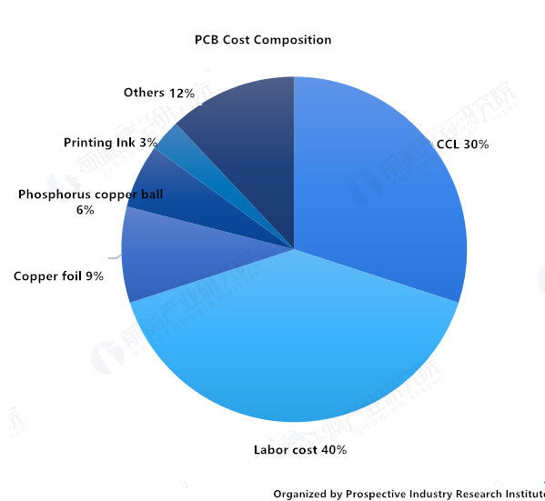
PCB relies heavily on upstream industries, especially copper-clad laminates (CCL). Copper-clad laminate is the highest cost of PCB single material, accounting for about 30% of the PCB cost.
Copper clad laminate (CCL), as a substrate material in PCB manufacturing, plays an important role in interconnection, conduction, insulation, and support of PCB, and has a great impact on signal transmission speed, energy loss, and characteristic impedance in the circuit. Therefore, the performance, quality, processability, manufacturing level, manufacturing cost, and long-term reliability and stability of printed circuit boards depend to a large extent on the copper-clad laminates.
At the same time, the copper-clad laminate has the strongest bargaining power in the upstream and downstream industrial chain structure. It not only has a strong voice in the purchase of raw materials such as fiberglass cloth and copper foil but also transfers the pressure of rising costs to downstream PCB manufacturers.
PCB is a bridge that carries electronic components and connects circuits. It is widely used in communication electronics, consumer electronics, computer, automotive electronics, industrial control, medical devices, national defense, aerospace, and other fields. The downstream industry has great traction and driving effect on the development of the PCB industry, and its demand changes directly determine the future development of the PCB industry.
The global PCB industry is growing slowly, and the industry continues to shift to China
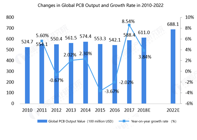
The Prismark data show that the global PCB output value in 2017 is about 58.84 billion US dollars, an increase of about 8.54% year on year. Prismark expects global PCB output value to reach about 68.81 billion US dollars by 2022.
In 2017, China's PCB output accounted for more than 50% of global PCB output. The compound growth rate of China's PCB output is estimated to be about 3.7% in 2017-2022, and it is estimated that China's PCB output will reach about 35.71 billion US dollars by 2022.
With the transfer of the global electronic information industry from developed countries to emerging economies and emerging countries, Asia, especially China, has gradually become the most important production base of electronic information products in the world. Before 2000, more than 70% of global PCB output value was distributed in the Americas (mainly North America), Europe, and Japan. Since the 21st century, the focus of the PCB industry has been shifting to Asia. At present, the output value of PCB in Asia has approached 90% of the world's total.
In recent years, the global economy is in a period of deep adjustment, and the leading role of major economies such as Europe, the United States, and Japan in world economic growth has been significantly weakened, while the degree of integration of China's global economy has been increasing, gradually occupying half of the global PCB market. As the largest producer of the PCB industry in the world, China's share of the global PCB industry's total output has increased from 31.18% in 2008 to 50.53% in 2017. The share of output in America, Europe, and Japan has declined sharply.
Environmental Pressure Accelerates Industry Integration and Industry Concentration Increases Continuously
China's PCB industry is too decentralized to limit the development of the industry, environmental protection policies will help upgrade the industry. At present, there are more than 2800 PCB enterprises in the world, while there are about 1500 in the mainland of China. They are mainly distributed in areas with a high concentration of electronic industry, large demand for basic components, and good transportation and water and electricity conditions, such as the Pearl River Delta, the Yangtze River Delta, and the Bohai Rim. The concentration of the PCB industry in China is too low, which severely limits the upgrading and development of the domestic PCB industry.
PCB will produce pollutants and noise such as waste gas, wastewater, and solid waste in the production process, which will have a greater impact on the lives of the surrounding residents. With the enhancement of national environmental awareness and the attention of national policies, the requirements of PCB production lines are becoming more and more stringent. After the Levy of environmental protection tax, the environmental protection requirements of the PCB industry are more stringent. It is estimated that the levy scale of environmental protection tax can reach 50 billion yuan annually.
The emission restriction policy reduces the living space of small factories and speeds up the elimination of backward production capacity within the industry, with an average of 5% of small factories cleared every year. Excluding low-quality capacity, market supply and demand will be more stable.
Large-scale PCB enterprises have established a sound plant pollution management system and equipment system. At the same time, only through continuous technological transformation and product upgrading can enterprises offset the cost of environmental protection investment. In the long run, the tightening of the policy will eliminate a large number of low-end products, backward technology production enterprises, to help improve the concentration of the industry. So that leading enterprises with advanced production technology to further bigger and stronger, thereby enhancing China's PCB industry in the global position.
New Demand Leads Industrial Upgrading, 5G Construction Drives PCB Volume and Price Rise
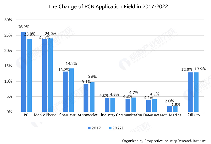
At present, the communication field is the largest downstream of PCB. According to Prismark data, in 2017, the output value of PCB in the global communication and electronics field reached 17.8 billion US dollars, accounting for 30.3% of the total output value of the global PCB industry. PCB downstream communications electronics market value of $567 billion in 2017, expected to maintain a compound growth rate of 2.9% over the next five years.
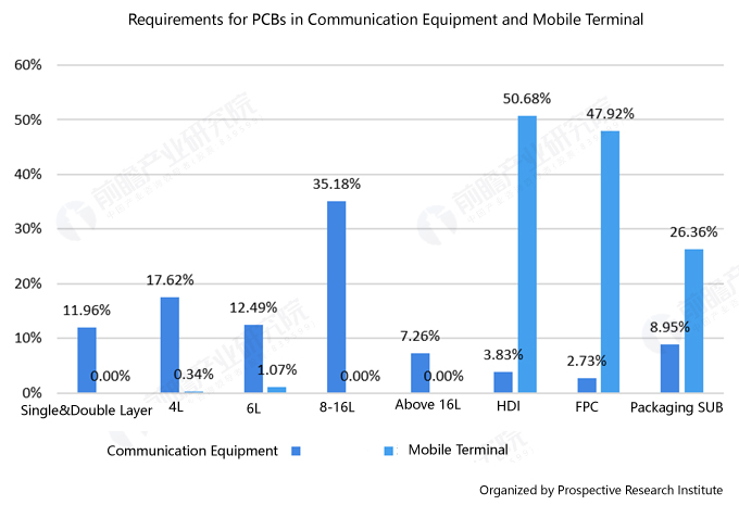
PCB demand for communication equipment is mainly high multi-layer board (8-16 layer board accounts for about 35.18%), and has 8.95% package substrate demand.
The application requirements of the PCB board in communication network construction are mainly in the four areas of wireless network, transmission network, data communication, and fixed network broadband. In the initial stage of 5G construction, the incremental demand for PCB is directly reflected in the wireless network and transmission network, and the demand for PCB backplane, high-frequency board, and high-speed multi-layer board is larger.
By the middle and later stages of 5G construction, with the rapid penetration of 5G high-bandwidth business applications, such as mobile high-definition video, vehicle networking, AR/VR, and other business applications, the data processing and exchange capacity of data centers will also have a greater impact. It is expected that after 2020, domestic data centers will be driven from 10G, 40G to 100G, 400G Super Large Data Center Upgrade, then the demand for high-speed multi-layer board in the data communication field will grow rapidly.
The arrival of 5G will have a tremendous impact on the telecommunication PCB industry. To sum up, on the one hand, the growth of "quantity" and on the other hand, the increase of technical difficulty will lead to the rise of "price".
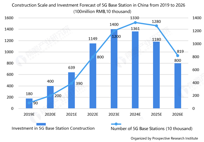
The number of 5G macro base stations is expected to exceed 5 million, and the number of micro base stations is expected to exceed 10 million. The 5G era will adopt the mode of "macro station + small station" network coverage. The transmission distance of the 5G base station using millimeter-wave is very short, and the coverage ability is greatly reduced. In order to reduce costs, the corresponding solution is to use a low-power "micro-base station". The cost of micro-base stations is low, and the radiation power is more uniform, which will become the mainstream technology in the future. According to the Ministry of Industry and Information Technology, the total number of 5G macro base stations will be about 1.2-1.5 times that of 4G base stations, which is expected to exceed 5 million, while the number of 5G micro base stations is conservatively estimated to be more than twice that of macro base stations.
Significant changes have taken place in the structure of 5G base stations. In the age of 5G communication, high-frequency and high-speed applications such as 5G high-frequency communication mobile phones, millimeter wave technology,
802.11ad high-speed WIFI has gradually become the new market demand. Under this premise, the upgrading demand for underlying electronic components such as PCB, FPC has also changed. The evolution of new processes and new materials
has become a future-defining trend for the electronics industry.
As the front-end receiving device of the base station, antenna, and radiofrequency require very low dielectric transmission loss and high thermal conductivity. More high-frequency CCL is needed. The number of high-frequency PCB boards used in
different frequency bands is different, and the unit value is about 1.5-2 times higher than that of FR-4 material used in 4G applications.
To sum up, the number of PCB boards required by a 5G single macro base station is 2.9 times that of 4G, and the value is expected to reach 134,000/station, which is 4.2 times that of a 4G base station.
According to the general plan of the Ministry of Industry and Information Technology, China's 5G network will start construction in the second half of 2019 and be put into commercial use in 2020. At present, the world has entered the 5G development stage. The market demand for high-speed, high-frequency, high-density, large-capacity PCB as the core components is growing rapidly. The core customers in the field of communications have clearly put forward the hope that the company's PCB products can synchronize with downstream technologies or even advance the development and rapidly enter the stage of industrialization.
We have reason to believe that the PCB industry will soon shine in the global 5G network peak.


