


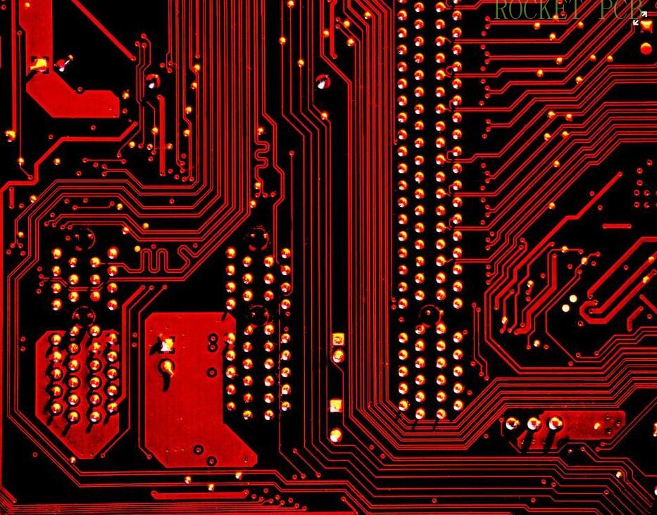
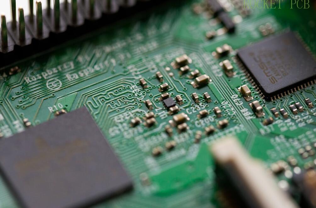
Summary of 66 common problems in high frequency PCB circuit design
In the design of high frequency PCB circuit, do you encounter the following problems?
1. How to select PCB board material ?
The choice of PCB board must strike a balance between meeting design requirements and mass production and cost. The design requirements include electrical and mechanical parts. This material problem is usually important when designing very high-speed PCB boards (frequencies greater than 10 GHz). For example, the current commonly used FR-4 material, the dielectric loss at several GHz frequency will have a great impact on the signal attenuation, which may not be used. As far as electricity is concerned, we should pay attention to whether the dielectric constant and dielectric loss are suitable at the designed frequency.
2. How to avoid high frequency interference?
The basic idea of avoiding high frequency interference is to minimize the interference of electromagnetic field of high frequency signal, which is called crosstalk. Increase the distance between high-speed signal and analog signal, or add ground guard / Mount traces beside analog signal. Attention should also be paid to the noise interference of digital ground to analog ground.
3. How to solve the problem of signal integrity in high speed design?
Signal integrity is basically a problem of impedance matching. The factors affecting impedance matching include the structure and output impedance of the signal source, the characteristic impedance of the wiring, the characteristics of the load end, and the topology architecture of the wiring. The solution is termination and routing topology adjustment.
4. How is the difference distribution line realized?
Two points should be paid attention to in the wiring of differential pairs. One is that the length of the two lines should be as long as possible. The other is that the distance between the two lines (which is determined by the differential impedance) should always remain unchanged, that is, to keep parallel. There are two ways of parallel: one is that two lines run on the same side by side, and the other is that two lines run on two adjacent layers (over under). In general, the former side-by-side (side-by-side) implementation is more.
5. For a clock signal line with only one output, how to realize the difference distribution line?
Only when the difference distribution line is used is the signal source and receiver are also differential signals. Therefore, the difference distribution line cannot be used for clock signal with only one output.
6. Can a matching resistance be added between the differential pairs at the receiving end?
The matching resistance between differential pairs at the receiving end is usually added, and its value should be equal to the value of differential impedance. So the signal quality will be better.
7. Why do differential pair routing be close and parallel?
The routing of differential pairs should be appropriately close and parallel. The so-called appropriate approach is because the distance will affect the value of differential impedance, which is an important parameter in the design of differential pairs. Parallel is also necessary because of the consistency of differential impedance. If the two lines are far or near, the differential impedance will be inconsistent, which will affect the signal integrity and timing delay.
8. How to deal with some theoretical conflicts in practical wiring?
Basically, it is right to separate and isolate the A / D ground. It should be noted that the signal wiring should not cross the moat as far as possible, and the return current path of power supply and signal should not be too large. Crystal oscillator is an analog positive feedback oscillation circuit. In order to have a stable oscillation signal, the specification of loop gain and phase must be met. However, the oscillation specification of the analog signal is easy to be interfered, even if ground guard traces are added, it may not be able to completely isolate the interference. Moreover, if it is too far away, the noise on the ground plane will also affect the positive feedback oscillation circuit. Therefore, the distance between the crystal oscillator and the chip must be as close as possible. Indeed, there are many conflicts between high-speed cabling and EMI requirements. But the basic principle is that the resistance and capacitance or ferrite beam added by EMI can not cause some electrical characteristics of the signal not to meet the specification. Therefore, it is better to solve or reduce EMI problems by arranging routing and PCB lamination, such as high-speed signal going through inner layer. Finally, resistance capacitance or ferrite beam is used to reduce the damage to the signal.
9. How to solve the contradiction between manual wiring and automatic wiring of high-speed signals?
At present, most of the strong automatic routing software have set constraints to control the winding mode and the number of vias. Sometimes, the setting items of winding engine capacity and constraints of various EDA companies are quite different. For example, whether there are enough constraints to control the way serpentine meanders, whether it can control the spacing of differential pairs and so on. This will affect whether the routing mode of automatic routing can meet the designer's idea. In addition, the difficulty of manually adjusting the wiring is absolutely related to the ability of the winding engine. For example, the push ability of the wire, the push ability of the through hole, and even the push ability of the wire to the copper coating, etc. Therefore, choosing a router with strong winding engine is the solution.
10. About test coupon.
Test coupon is used to measure whether the characteristic impedance of PCB meets the design requirements by TDR (time domain reflector). Generally, there are two kinds of impedance to be controlled: single wire and differential pair. Therefore, the line width and line spacing (with differential pairs) on the test coupon should be the same as the lines to be controlled. The most important thing is the location of the ground point when measuring. In order to reduce the inductance value of the ground lead, the place where the TDR probe is grounded is usually very close to the place where the signal is measured (probe tip). Therefore, the distance and mode between the measuring signal point on the test coupon and the grounding point should be in accordance with the probe used.
11. In the design of high-speed PCB, the blank area of signal layer can be coated with copper. How to distribute the copper coating of multiple signal layers on grounding and power supply?
Generally, the copper coating in the blank area is mostly grounded. The distance between the copper coating and the signal line should be paid attention to when copper is deposited beside the high-speed signal line, because the copper coating will reduce the characteristic impedance of the line a little bit. It should also be noted that the characteristic impedance of other layers should not be affected, such as in the structure of dual strip line.
12. Can the microstrip line model be used to calculate the characteristic impedance of the signal line above the power plane?
Can the signal between power supply and ground plane be calculated using stripline model?Yes, when calculating the characteristic impedance, both the power plane and the ground plane must be regarded as the reference plane. For example, four layer board: top layer power layer layer layer bottom layer, then the model of characteristic impedance of top layer is microstrip line model with power plane as reference plane.
13. Can test points be automatically generated by software on high-density PCB, which can meet the test requirements of mass production in general?
Whether the test points generated automatically by general software meet the test requirements or not depends on whether the specifications of the test points meet the requirements of the test equipment. In addition, if the wiring is too dense and the specification of adding test points is relatively strict, it may not be possible to automatically add test points to each section of the line. Of course, the test points need to be manually supplemented.
14. Will adding test points affect the quality of high-speed signals?
As for whether the signal quality will be affected depends on the way to add test points and how fast the signal is. Basically, additional test points (not via or dip pins) may be added to or pulled out of the line. The former is equivalent to adding a very small capacitance on the line, while the latter has an extra branch. Both of these two conditions will affect the high-speed signal to some extent. The degree of influence is related to the frequency speed and edge rate of the signal. The magnitude of the influence can be obtained by simulation. In principle, the smaller the test point is, the better (of course, it must meet the requirements of the test machine), and the shorter the branch, the better.
15. How to connect the ground wires between several PCB systems?
When the signals or power supply between the PCB boards are in action, for example, board a has power supply or the signal is sent to board B, there must be an equal amount of current flowing back from the formation to the board a (this is Kirchoff current law). The current in this formation will flow back to the place with the least impedance. Therefore, the number of pins allocated to the formation should not be too small at each interface where the power supply or signal are connected to each other, so as to reduce the impedance, so as to reduce the noise on the formation. In addition, we can also analyze the whole current loop, especially the part with large current, adjust the grounding method of the stratum or ground wire to control the current path (for example, make a low impedance somewhere to let most of the current go from this place), and reduce the impact on other sensitive signals.
16. Can you introduce some foreign technical books and data about high speed PCB design?
At present, the application of high-speed digital circuit has communication network and calculator and other related fields. In terms of communication network, the working frequency of PCB board has reached up to and below GHz, and as far as I know, there are as many as 40 layers. Calculator related applications also because of the progress of the chip, whether it is a general PC or server (server), the highest operating frequency on the board has reached 400MHz (such as Rambus). In response to this high-speed and high-density routing requirements, blind / buried vias, mircrovias and build-up processes are increasingly needed. These design requirements can be mass produced by manufacturers.
17. Two commonly used characteristic impedance formulas are as follows:
z = {87 / [sqrt (ER + 1. 41)]} ln [5. 98h / (0. 8W + T)], where W is the line width, t is the thickness of copper sheet, h is the distance from the line to the reference plane, and ER is the dielectric constant of PCB material. This formula can only be applied when 0. 1 < (w / h) < 2. 0 and 1 < (ER) < 15. Stripline z = [60 / sqrt (ER)] ln {4H / [0. 67 π (T + 0. 8W)]} where h is the distance between the two reference planes, and the trace is located in the middle of the two reference planes. This formula can only be applied when w / h < 0. 35 and T / h < 0. 25.
18. Can ground wire be added in the middle of differential signal line?
In general, ground wire cannot be added in the middle of differential signal. Because the application principle of differential signal is the most important point is to use the advantages of coupling between differential signals, such as flux cancellation, noise immunity ability and so on. If a ground wire is added in the middle, the coupling effect will be destroyed.
19. Does rigid and flexible board design require special design software and specifications?
Where can we undertake this kind of PCB processing in China?Flexible printed circuit can be designed with general PCB design software. The Gerber format is also used for FPC manufacturers. Because the manufacturing process is different from general PCB, each manufacturer will limit the minimum line width, minimum wire spacing and minimum aperture (via) according to their manufacturing capacity. In addition, some copper sheets can be laid at the turning point of the flexible circuit board for reinforcement. As for the manufacturers, they can go online to "FPC", when the keyword query should be found.
20. What is the principle of proper selection of grounding point between PCB and enclosure?
The selection principle of PCB and shell grounding point selection is to provide low impedance path to return current and control the return current path. For example, in the vicinity of high-frequency devices or clock generators, the floor of PCB can be connected with chassis ground by fixed screws, so as to minimize the area of the whole current loop and reduce electromagnetic radiation.
21. What aspects should debug of circuit board start from?
In terms of digital circuits, first of all, determine three things in order: 1) make sure that all power values meet the design requirements. Some systems with multiple power sources may require that the order and speed of some power supplies rise up to a certain standard. 2) Make sure that all clock signal frequencies are working properly and that there is no non monotonic problem on the signal edge. 3) Confirm whether the reset signal meets the specification requirements. If these are normal, the chip should send out the signal of the first cycle. Next, debug according to the system operation principle and bus protocol.
22. When the size of the circuit board is fixed, if more functions need to be accommodated in the design, it is often necessary to improve the routing density of PCB. However, this may lead to the enhancement of mutual interference of the wiring. At the same time, if the wiring is too thin, the impedance cannot be reduced. Please introduce the skills in the design of high-speed (> 100MHz) high-density PCB?
When designing high-speed and high-density PCB, crosstalk interference should be paid special attention to because it has great influence on timing and signal integrity. The following provides several points for attention: control the continuity and matching of the characteristic impedance of the wiring: the size of the wiring spacing. Generally, the spacing is twice the line width. Through simulation, we can know the influence of routing spacing on timing and signal integrity, and find out the minimum tolerable spacing. The results of different chip signals may be different. Choose the appropriate termination method: avoid the same routing direction between the upper and lower adjacent layers, and even overlap the upper and lower layers, because the crosstalk is greater than that of adjacent lines in the same layer. Blind / buried via (blind / buried via) was used to increase the routing area. But the production cost of PCB board will increase. In practice, it is very difficult to achieve full parallelism and isometric, but we should try our best. In addition, differential termination and common mode termination can be reserved to mitigate the impact on timing and signal integrity.
23. LC circuit is often used for filtering at analog power supply. But why sometimes LC filter is worse than RC filter?
The comparison of LC and RC filtering results must consider whether the selection of frequency band and inductance value to be filtered out is appropriate. Because the inductance of inductance is related to inductance value and frequency. If the noise frequency of the power supply is low and the inductance value is not large enough, the filtering effect may not be as good as that of RC. However, the cost of using RC filter is that the resistance itself will consume energy and the efficiency is poor, and attention should be paid to the power that the selected resistor can bear.
24. What is the method of selecting inductance and capacitance in filtering?
In addition to the noise frequency to be filtered out, the response ability of instantaneous current should be considered in the selection of inductance value. If the output of LC will have the opportunity to output large current instantaneously, too much inductance will hinder the speed of the large current flowing through the inductor and increase ripple noise. The capacitance is related to the allowable ripple noise. The smaller the ripple noise, the larger the capacitance. The ESR / ESL of capacitance also has an effect. In addition, if the LC is placed at the output of the switching regulation power supply, we should also pay attention to the influence of the pole / zero produced by the LC on the stability of the negative feedback control loop.
25. How to meet the requirements of EMC as much as possible without causing too much cost pressure?
The increased cost of PCB due to EMC is usually due to the increase of the number of layers to enhance the shielding effect and the addition of ferrite beam, choke and other high-frequency harmonic suppression devices. In addition, the shielding structure on other institutions is usually required to make the whole system pass the EMC requirements. The following only provides a few PCB design skills to reduce the electromagnetic radiation effect produced by the circuit. The device with slow slope rate should be selected as far as possible to reduce the high frequency component generated by the signal. Pay attention to the location of high frequency devices, and do not close to the external connector. Pay attention to impedance matching of high-speed signal, routing layer and return current path to reduce high-frequency reflection and radiation. Sufficient and appropriate decoupling capacitors are placed on the power pins of each device to mitigate the noise on the power supply layer and the formation. Pay special attention to whether the frequency response and temperature characteristics of the capacitor meet the design requirements. The ground near the external connector can be properly separated from the stratum, and the ground of the connector can be connected to the chassis ground nearby. Ground guard / Mount traces can be properly used beside some special high-speed signals. But we should pay attention to the influence of guard / Mount traces on the characteristic impedance. The power source layer is 20 h smaller than that of the formation, and H is the distance between the power source layer and the formation.
26. When there are multiple D / a function blocks in a PCB, the conventional method is to separate the D / a ground. Why?
The reason of separating digital from analog ground is that the digital circuit will generate noise in the power supply and generated when switching between high and low potential. The noise level is related to the speed and current of the signal. If the ground plane is not divided and the noise generated by the digital area circuit is large and the analog area circuit is very close, even if the digital and analog signals are not crossed, the analog signal will still be interfered by the ground noise. In other words, the method of digital analog ground separation can only be used when the analog circuit area is far away from the digital circuit area which produces large noise.
27. Another method is to ensure that the digital / analog is separated and the digital / analog signal lines are not crossed. The whole PCB board is not divided and the digital / analog ground is connected to this ground plane. What is the reason?
The requirement that the digital and analog signal wiring cannot be crossed is that the return current path of a slightly faster digital signal will flow back to the source of the digital signal along the ground near the bottom of the wiring as far as possible. If the digital and analog signal wiring is crossed, the noise generated by the return current will appear in the analog circuit area.
28. How to consider impedance matching in high speed PCB schematic design?
In the design of high-speed PCB circuit, impedance matching is one of the design elements. The impedance value is absolutely related to the wiring mode, such as walking on the surface layer (microstrip) or inner layer (stripline / double stripline), the distance from the reference layer (power layer or stratum), the wiring width, PCB material, etc. , will affect the characteristic impedance value of the wiring. That is to say, the impedance value can only be determined after wiring. Due to the limitation of the line model or the mathematical algorithm used, the general simulation software can not consider some impedance discontinuities. At this time, only some terminators (such as series resistance) can be reserved on the schematic diagram to alleviate the effect of the impedance discontinuity. The real way to solve the problem is to avoid impedance discontinuity when wiring.
29. Where can we provide a more accurate IBIS model library?
The accuracy of IBIS model directly affects the simulation results. Basically, Ibis can be regarded as the electrical characteristic data of the I / obuffer equivalent circuit of the actual chip, which can be converted from SPICE model (measurement can be used, but there are many restrictions). The spice data is absolutely related to the chip manufacturing. Therefore, the spice data of the same device provided by different chip manufacturers are different, and the converted IBIS model data will also followDifferent. That is to say, if the devices of manufacturer a are used, only they have the ability to provide accurate model data of their devices, because no one else knows better than them what process their devices are made of. If the Ibis provided by the manufacturer is not accurate, the fundamental solution is to ask the manufacturer to improve continuously.
30. In high-speed PCB design, what aspects should designers consider the rules of EMC and EMI?
In general, both radiated and conducted aspects should be considered in EMI / EMC design. The former belongs to the higher frequency part (> 30MHz), while the latter belongs to the lower frequency part (< 30MHz). So we can’t only pay attention to the high frequency and ignore the low frequency part. A good EMI / EMC design must consider the location of devices, the arrangement of PCB stack, the way of important on-line and the selection of devices at the beginning of layout. If there is no better arrangement in advance, the solution after the event will get twice the result with half the effort and increase the cost. For example, the position of clock generator should not be close to the external connector, the high-speed signal should go through the inner layer as much as possible and pay attention to the characteristic impedance matching and the continuity of the reference layer to reduce the reflection. The slope rate of the signal pushed by the device should be as small as possible to reduce the high-frequency component. When selecting the decoupling / bypass capacitor, pay attention to whether the frequency response meets the requirements to reduce the noise of the power layer. In addition, attention should be paid to the return path of high-frequency signal current to make the loop area as small as possible (that is, the loop impedance loop impedance should be as small as possible) to reduce radiation. The range of high frequency noise can also be controlled by dividing strata. Finally, the proper choice of PCB and the chassis ground.
31. How to choose EDA tools?
In the current PCB design software, thermal analysis is not a strong point, so it is not recommended to use it. Other functions 1. 3. 4 can be selected as pads or cadence, and the performance price ratio is good. PLD design beginners can use the integrated environment provided by PLD chip manufacturers, and can choose single point tools when designing more than one million gates.
32. Please recommend an EDA software suitable for high speed signal processing and transmission.
In the conventional circuit design, the pads of innoveda is very good, and there are simulation software for it, and this kind of design often occupies 70% of the applications. In high-speed circuit design, analog and digital mixed circuit, cadence’s solution should belong to the software with better performance and price. Of course, mentor’s performance is very good, especially its design process management should be the best.
33. Explain the meaning of each layer of PCB board?
Topoverlay: the name of the top-level device, also known as top silksscreen or top component legend, such as R1, C5, IC10. Bottom overlay. Similarly, multilayers: if you design a 4-layer board, you place a free pad or via and define it as a multilay, then its pad will automatically appear on the four layers. If you only define it as top layer, then its pad will only appear on the top layer.
34. 2G above high frequency PCB design, wiring, typesetting, what should be paid attention to?
High frequency PCB above 2G belongs to RF circuit design, which is not in the scope of high-speed digital circuit design. The layout and routing of RF circuit should be considered together with schematic diagram, because both layout and routing will cause distribution effect. Moreover, some passive components in RF circuit design are realized by parametric definition and special shape copper foil. Therefore, EDA tools are required to provide parametric devices and edit special shape copper foil. The Board Station of mentor company has special RF design module, which can meet these requirements. In addition, the general RF design requires special RF circuit analysis tools. The most famous tool in the industry is Agilent’s eesoft, which has a good interface with mentor’s tools. What rules should be followed in the design of high frequency PCB with
35. What rules should be followed in the design of microstrip for high frequency PCB design above 2G?
The design of RF microstrip line requires 3D field analysis tools to extract transmission line parameters.
All rules should be specified in this field extraction tool.
36. For PCB with full digital signal, there is an 80 MHz clock source on the board. In addition to the use of wire mesh (grounding), in order to ensure that there is enough driving capacity, what kind of circuit should be used for protection?
To ensure the driving ability of the clock, it should not be realized by protection. Generally, the clock driver chip is used. The general concern about clock drive capability is due to multiple clock loads. The clock driver chip is used to change a clock signal into several, and point-to-point connection is adopted. In order to select the driver chip, in addition to ensuring the basic matching with the load, the signal edge meets the requirements (generally, the clock is the edge effective signal). When calculating the system timing, the clock delay in the driver chip should be included.
37. If a separate clock signal board is used, what kind of interface is generally used to ensure that the transmission of clock signal is less affected?
The shorter the clock signal, the smaller the transmission line effect. Using a separate clock signal board will increase the length of signal wiring. And the grounding power supply of the single board is also a problem. If long distance transmission is needed, differential signal is recommended. LVDS signal can meet the requirements of driving capacity, but your clock is not too fast, so it is unnecessary.
38. 27m, SDRAM clock lines (80m-90m). The second and third harmonics of these clock lines are just in VHF band, and the interference is very large after high frequency channeling into the receiver. In addition to shortening the length of the line, are there any other good ways?
If the third harmonic is large and the second harmonic is small, it may be because the duty cycle of the signal is 50%, because in this case, the signal has no even harmonics. The duty cycle of the signal needs to be modified. In addition, if the clock signal is unidirectional, the source end series matching is generally used. This can suppress the secondary reflection, but does not affect the clock edge rate.
39. What is the routing topology?
Topology, also known as routing order, refers to the routing order of multi port connected networks.
40. How to adjust the routing topology to improve signal integrity?
This kind of network signal direction is more complex, because for one-way, two-way signals, different levels of signals, the impact of topology is different, it is difficult to say which topology is good for signal quality. In the pre simulation, engineers are required to know the circuit principle, signal type and even wiring difficulty.
41. How to reduce EMI by stacking?
First of all, EMI should be considered from the system, PCB alone can not solve the problem. In my opinion, it is the worst way to reduce the interference area of the signal. In addition, the tight coupling between the formation and the power layer is beneficial to the suppression of common mode interference.
42. Why laying copper?
There are several reasons for laying copper. 1) EMC. For a large area of ground or power supply copper, will play a shielding role, some special, such as PGND play a protective role. 2) PCB process requirements. Generally, in order to ensure the electroplating effect, or the laminate does not deform, copper is laid on the PCB with less wiring. 3) Signal integrity requires a complete return path for high-frequency digital signals, and reduces the wiring of DC network. Of course, there are heat dissipation, special device installation requirements copper and other reasons.
43. In a system, DSP and PLD are included. What problems should be paid attention to when wiring?
Look at the ratio of your signal rate to the length of the wiring. If the time delay of the signal on the transmission line and the time along the signal change are comparable, the problem of signal integrity should be considered. In addition, for multiple DSP, clock, data signal routing, Topp will also affect the signal quality and timing, which needs to be paid attention to.
44. Are there any other good tools besides Protel tools for wiring?
In addition to Protel, there are many wiring tools, such as mentor’s wg2000, en2000 series and powerpcb, cadence’s Allegro, zuken’s cadstar, cr5000, etc. each has its own advantages.
45. What is the "signal return path"?
Signal return path, i. e. return current. When the high-speed digital signal is transmitted, the signal flows from the driver along the PCB transmission line to the load, and then the load returns to the driver through the shortest path along the ground or power supply. This return signal on the ground or power supply is called the signal return path. Dr. JohsonIn his book, he explains that high-frequency signal transmission is actually the process of charging the dielectric capacitor sandwiched between the transmission line and the DC layer. Si analyzes the electromagnetic characteristics of the enclosure and the coupling between them.
46. How to do SI analysis for plug-ins?
In ibis3. 2 specification, there is a description of the plug-in model. Generally, EBD model is used. For special boards, such as backplanes, SPICE models are required. Multi board simulation software (HyperLynx or is) can also be used_When establishing a multi board system, input the distribution parameters of the connector, which are generally obtained from the plug-in manual. Of course, this method will not be accurate enough, but only within the acceptable range.
47. What are the termination methods?
Termination, also known as matching. Generally, according to the matching position, it can be divided into active end matching and terminal matching. The source end matching is generally resistance series matching, terminal matching is generally parallel matching, there are more ways, including resistance pull-up, resistance pull-down, Davidson matching, AC matching, Schottky diode matching.
48. What factors determine the method of termination (matching)?
The matching mode is generally determined by the characteristics of the buffer, the top situation, the type of level and the mode of decision. The duty cycle of the signal and the power consumption of the system should also be considered.
49. What are the rules of termination (matching)?
The most important problem of digital circuit is timing. The purpose of adding and matching is to improve the signal quality and get the signal that can be determined at the time of decision. For the level effective signal, the signal quality is stable under the premise of ensuring the establishment and holding time; for the delay effective signal, the signal change delay speed meets the requirements under the premise of ensuring the signal delay monotonicity. There are some materials about matching in mentor ICX product textbook. In addition, "high speed digital design a hand book of blackmagic" has a chapter dedicated to terminal, which describes the effect of matching on signal integrity from the principle of electromagnetic wave for reference.
50. Can the IBIS model be used to simulate the logic function of the device? If not, how to simulate the circuit at board level and system level?
IBIS model is a behavior level model and cannot be used in functional simulation. SPICE model or other structure level model is needed for functional simulation.
51. In the system of digital and analog coexisting, there are two processing methods: one is to separate the digital and the analog. For example, in the stratum, the digital ground is independent, and the analog ground is independent. The single point is connected with copper sheet or FB magnetic bead, but the power supply is not separated; the other is that the analog power source and digital power source are separately connected by FB, and the ground is unified. Is the effect of the two methods the same?
It should be said that it is the same in principle. Because power and ground are equivalent to high frequency signals. The purpose of distinguishing analog and digital parts is to resist interference, mainly the interference of digital circuit to analog circuit. However, segmentation may cause incomplete signal return path, affect the signal quality of digital signal and the EMC quality of the system. Therefore, no matter which plane is divided, it depends on whether the signal return path is increased and how much interference the return signal has on the normal working signal. Now there are some hybrid designs, regardless of power supply and ground. In the layout, the digital part and the analog part are separately arranged to avoid cross region signal.
52. Safety regulation: what are the specific meanings of FCC and EMC?
FCC:federal communication American Communications CommissionEMC:electro megnetic Compatibility EMC FCC is a standard organization, EMC is a standard. There are corresponding reasons for the promulgation of standards, standards and test methods.
53. What is the difference distribution line?
Differential signal, some also known as differential signal, uses two identical, opposite polarity signals to transmit one channel of data, depending on two signal level difference for judgment. In order to ensure that the two signals are completely consistent, the line width and line spacing should be kept unchanged during wiring.
54. What are the PCB simulation software?
There are many kinds of simulation, such as ICX, signalvision, HyperLynx, xtk, spectraquest, etc. Some also use HSPICE.
55. How does PCB simulation software perform layout simulation?
In high-speed digital circuit, in order to improve the signal quality and reduce the difficulty of wiring, multilayer board is generally used to distribute special power layer and stratum.
56. How to ensure the stability of signals above 50m in layout and wiring?
The key of high-speed digital signal wiring is to reduce the influence of transmission line on signal quality. Therefore, the signal routing should be as short as possible when the high-speed signal layout is more than 100m. In digital circuit, high speed signal is defined by the rise delay time of signal. Moreover, different kinds of signals (such as TTL, GTL, LVTTL) have different methods to ensure signal quality.
57. The RF part, intermediate frequency part and even low frequency circuit part of outdoor unit monitoring are often deployed on the same PCB. What are the material requirements for such a PCB?
How to prevent interference between RF, if and LF circuits? Hybrid circuit design is a big problem. It’s hard to have a perfect solution. In general, RF circuits are placed and wired as an independent single board in the system, and even have a special shielding cavity. And the RF circuit is generally single-sided or double-sided board, the circuit is relatively simple, all these are to reduce the impact on the distribution parameters of RF circuit and improve the consistency of RF system. Compared with the common FR4 material, the RF circuit board tends to adopt the substrate with high Q value. The dielectric constant of the material is relatively small, the distributed capacitance of the transmission line is small, the impedance is high, and the signal transmission delay is small. In the hybrid circuit design, although RF and digital circuits are on the same PCB, they are generally divided into RF circuit area and digital circuit area, which are laid and wired separately. Ground through hole tape and shielding box are used for shielding.
58. For the RF part, if part and low frequency circuit part are deployed on the same PCB, what solution does mentor have?
In addition to the basic circuit design function, mentor’s board level system design software also has special RF design module. In RF schematic design module, parametric device model is provided, and bidirectional interface with eesoft and other RF circuit analysis and simulation tools is provided. The layout module provides the pattern editing function for RF circuit layout and wiring. It also has a bidirectional interface with eesoft and other RF circuit analysis and simulation tools. The analysis and simulation results can be marked back to the schematic diagram and PCB. At the same time, using the design management function of mentor software, design reuse, design derivation and collaborative design can be realized conveniently. The process of hybrid circuit design is greatly accelerated. Mobile phone board is a typical hybrid circuit design. Many large mobile phone design manufacturers use mentor and angelen’s eesoft as the design platform.
59. On a 12 layer PCB board, there are three power supply layers of 2. 2V, 3. 3V and 5V. How to deal with the ground wire when the three power supplies are in one layer respectively?
Generally speaking, the three power supplies are respectively made in three layers, which is better for signal quality. Because it is unlikely that the signal will be segmented across the plane layer. Cross segmentation is a key factor affecting signal quality, which is generally ignored by simulation software. It is equivalent to high frequency signal for both power source layer and formation. In practice, in addition to the consideration of signal quality, power plane coupling (using adjacent ground plane to reduce the AC impedance of power plane) and laminated symmetry are all factors to be considered.
60. How to check whether the PCB meets the design process requirements when leaving the factory?
Many PCB manufacturers have to go through the power on and off test before PCB processing and leaving the factory to ensure that all wiring is correct. At the same time, more and more manufacturers also use X-ray test to check some faults in etching or lamination. For the finished board after chip processing, ICT test is generally used, which requires adding ICT test points in PCB design. If there is a problem, a special X-ray inspection equipment can also be used to eliminate whether the processing causes the fault.
61. Do we need to consider the ESD problem of the chip itself when choosing the chip?
Whether it is a double-layer plate or a multi-layer board, the area of the ground should be increased as much as possible. ESD characteristics of the chip itself should be considered when selecting a chip, which is generally mentioned in the chip description, and even if the same chip from different manufacturers has different performance. More attention should be paid to the design, and the performance of the circuit board will be guaranteed. However, ESD problems may still occur, so the protection of the organization is also very important for ESD protection.
62. In order to reduce the interference when making PCB, should the ground wire form a closed sum form?
When making PCB board, generally speaking, the circuit area should be reduced in order to reduce the interference. When laying the ground wire, it should not be arranged in a closed form, but should be arranged in a tree shape, and the area of the ground should be increased as much as possible.
63. If the emulator uses one power supply and the PCB uses one power supply, should the ground of the two power supplies be connected together?
If you can use separate power supply, of course, because it is not easy to produce interference between power supplies, but most of the equipment has specific requirements. Since the emulator and PCB board use two power supplies, in my opinion, they should not be shared.
64. A circuit is composed of several PCB boards. Should they be grounded together?
A circuit is composed of several PCBs, most of which require common ground, because it is not practical to use several power supplies in one circuit. But if you have specific conditions, you can use different power supply, of course, the interference will be less.
65. Design a handheld product with LCD and metal shell. When testing ESD, it can not pass ice-1000-4-2 test, contact can only pass 1100V, air can pass 6000V. In ESD coupling test, horizontal can only pass 3000V, vertical can pass 4000V test. The main frequency of CPU is 33MHz. Is there any way to pass ESD test?
Hand held products are metal shell, ESD problem must be more obvious, LCD may appear more bad phenomenon. If there is no way to change the existing metal material, it is suggested to add anti electricity material inside the mechanism to strengthen the PCB grounding, and at the same time, try to make LCD grounding. Of course, how to operate depends on the specific situation.
66. When designing a system with DSP and PLD, which aspects should ESD be considered?
As for general system, it is necessary to consider the part directly contacted by human body, and carry out appropriate protection on circuit and mechanism. How much ESD will affect the system depends on the situation. In dry environment, ESD phenomenon will be more serious, the effect of ESD will be relatively obvious in sensitive and fine system. Although the ESD effect of large system is not obvious sometimes, more attention should be paid in the design to prevent the occurrence of ESD.


