


Analyzing Glass PCB - Everything you want to know
Introduction
In our daily lives, using plenty of appliances is widespread, and all these appliances are provided with PCBs. Hence, you can safely assume that PCBs are a significant innovation. Well, when it comes to these circuit boards, the primary consideration is the material it is made up of and how is that material integrated to create a glass PCB.
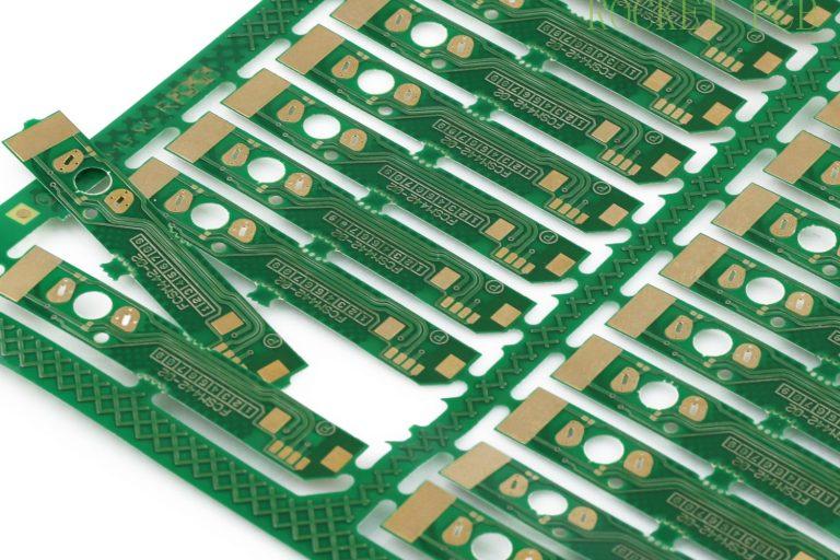
The usual PCBs are made using copper boards layered and printed with the components over them. However, nowadays, there is another kind of PCB, which is the glass PCB.
What is Glass PCB?
Glass PCB is rare since it is not used on many appliances; however, certain products like LCDs and other optical devices are commonly equipped with this PCB. However, in the case of a glass PCB, a UV-curable mask is used to transfer the circuit to the copper board.
The glass substrate used in a glass PCB is ideal for appliances that need stability with thermal materials. A board is first designed so the circuit can be printed, and the material used to manufacture the board is copper.
A technique for removing excess copper is then used, which is known as etching. A curable mask of UV will be needed to relocate the circuit to the glass material in a PCB. The entire procedure used ultraviolet light to manufacture the glass PCB.
Materials needed to make Glass PCB
There are certain materials that will be needed to manufacture a glass PCB, and these materials are listed below:
● Glass for the circuit
● Iron chloride
● Baking soda
● Copper foil
● UV photo resistance
● Glue for sticking
● Circuit layout in the form of OHP printout
Glass PCB circuit layout
The circuit board's layout is first printed on an OHP printer to have a design. Once the circuit board diagram is created, the layout of the glass PCB is drafted. A tool that automatically routes the circuit is then used to create the entire route.
Once the software creates the design, the picture is saved in PNG format. The areas on the copper foil that are required to be kept are subjected to photoresist, and these areas will be left behind.
After this, some of the steps are further followed, and these include the following:
Printed Layout
The purpose of using an OHP print is because this paper has the capability to block the UV light from passing on the areas that are not part of the circuit. Hence, by way of this, the desired areas are transparent, and UV light passes through them.
Glass glue to copper foil
Now, the copper has to be glued to the glass, and after gluing, the iron chloride will be used so that the copper is dissolved within the glass after its application. The thicker the copper foil is, the more time it will take to dissolve. It is better to choose the thickness of copper around 0.05mm.
The task of cleaning the foil of copper is the initial step when using rubbing alcohol; the copper is cleaned so that it doesn't stick to it with rigidity. Some glue is applied to the glass, and the copper foil is attached correctly, leaving no air bubbles.
Using photoresist
The next step is sticking the photoresist material on the copper foil. The photoresist material is very adhesive, so it must be handled carefully. When removed from the photoresist material, the cover must be immediately stuck to the copper board.
Modifying Exposure Settings
Now over the photoresist material, which is attached to the copper board, the placement of the OHP printout over the copper board is done. In this step, it is imperative to ensure that the side on which the OHP print is placed is the correct one, and then it has to let it get exposed to the UV light.
Illumination
The next step is subjecting the entire setup to the light. This may be UV sunlight, or an artificial UV light source can also be used. The exposure is suitable for around 5 minutes only. It's imperative that the entire setup stays stable throughout the exposure process. Now, after you have exposed it to UV light for 5 minutes, you can remove everything now.
Creating resistance
Removing the layer on the resist film is needed now, which you can do with scotch tape. Now, a baking soda solution is made, and the circuit board is dipped in it until the excess material washes away, leaving behind the circuit's track.
Etching
In the final step, the etching is carried out by dissolving the iron chloride into water. This solution is then used to dip the copper board, washing away all the excess copper on the board. The pathways of the circuit will be evident and visible on the board now.
Advantages of Glass PCB
There are many applications of glass PCB, like in 5G, LCD, LED, and several other appliances that need a transparent circuit board due to their layout.
There are many advantages of a glass PCB, and some of these are provided below:
● Due to the nature of glass, it doesn't deform when the appliances are subjected to high heat and pressure, so it is durable in such appliances.
● It has a flat surface and is transparent, so it is suitable to be easily adjusted into many appliances.
● A glass PCB won't require a heat sink.
● It offers tear resistance as well as is resistant to heat.
● Any chemicals don't damage the glass PCB; hence it proves to be quite chemical resistant.
● The issue of light attenuation does not exist in the glass PCB.
Conclusion
Glass PCBs require a very detailed and extensive procedure that has many steps in the process of manufacturing. So, when it comes to having the best glass PCBs, you can always choose Rocket PCB.
We provide the best PCBs worth choosing and have a very detailed circuit pattern over them. These glass PCBs can be used in various appliances you might be manufacturing. Especially such appliances that need a very high heat-resistant PCB may find a glass PCB the right choice compared to other options.
So get in touch with us today and have your hands on the best quality glass PCBs manufactured after a detailed analysis.


