
English


You are not just looking for a PCB supplier...
In Rocket PCB, one cooperation means lifelong cooperation service. We rely on quality and service to spread word-of-mouth. Professional and refined service to let you not only find a PCB maker, but also a reassured, reliable PCB partner to let you worry-free.
Before standard PCB production, when you develop a new PCB-based design, you may go through many design iterations. You need to be able to quickly test your new design in order to complete production in time, as the long design process can lead to loss of revenue. The rapid speed of our PCB prototype services, combined with test design before standard production runs, minimizes wasted project spending and maximizes your investment.
The earlier you discover design defects or inefficiencies in a PCB design, the lower the cost of solving the problem. If you don't use prototype PCB boards to test the design, you may have problems later in production, that is, after you invest a lot of money to produce standard PCB. Small batch production also applies to our PCB prototyping service.
The biggest advantage of Rocket PCB is that there is no MOQ and no matter what type of PCB, it is very easy for us.
Maybe you are worried about the PCB prototyping production of the high-end board you designed because only one PCB supplier has a limited production capacity and cannot meet the diverse needs. Or you can’t find a supplier that matches you due to the high barriers to entry for high-end factories. However, we can support high-end boards such as HDI PCB, high-frequency PCB, hybrid materials PCB, rigid-flex boards, and there is no minimum order quantity. Behind us are world-class PCB suppliers, such as Shennan circuit, Shengyi electronic, Suntek, Fastprint, Q & D, Sunshine, Delton, Fastpcb, Bomin., etc.
Through our professional service, your products can be put into production quickly and efficiently. We comprehensively control the quality of products and follow up on the delivery date, so that you have no worries. Through our services, your PCB sample prototyping work becomes simple, so that you can get cheaper prices, the most intimate service, and quality assurance.
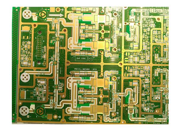
The difference between multilayer PCB board manufacturing and double layers PCB manufacturing is that lamination technology is needed, and the process is much more. The average manufacturing layers of Rocket PCB is as high as 8-20 layers, and the highest level is 64 layers. In the inner layer production and lamination technology to achieve a very high level. The thickness to diameter ratio (thickness diameter ratio) is 16:1.
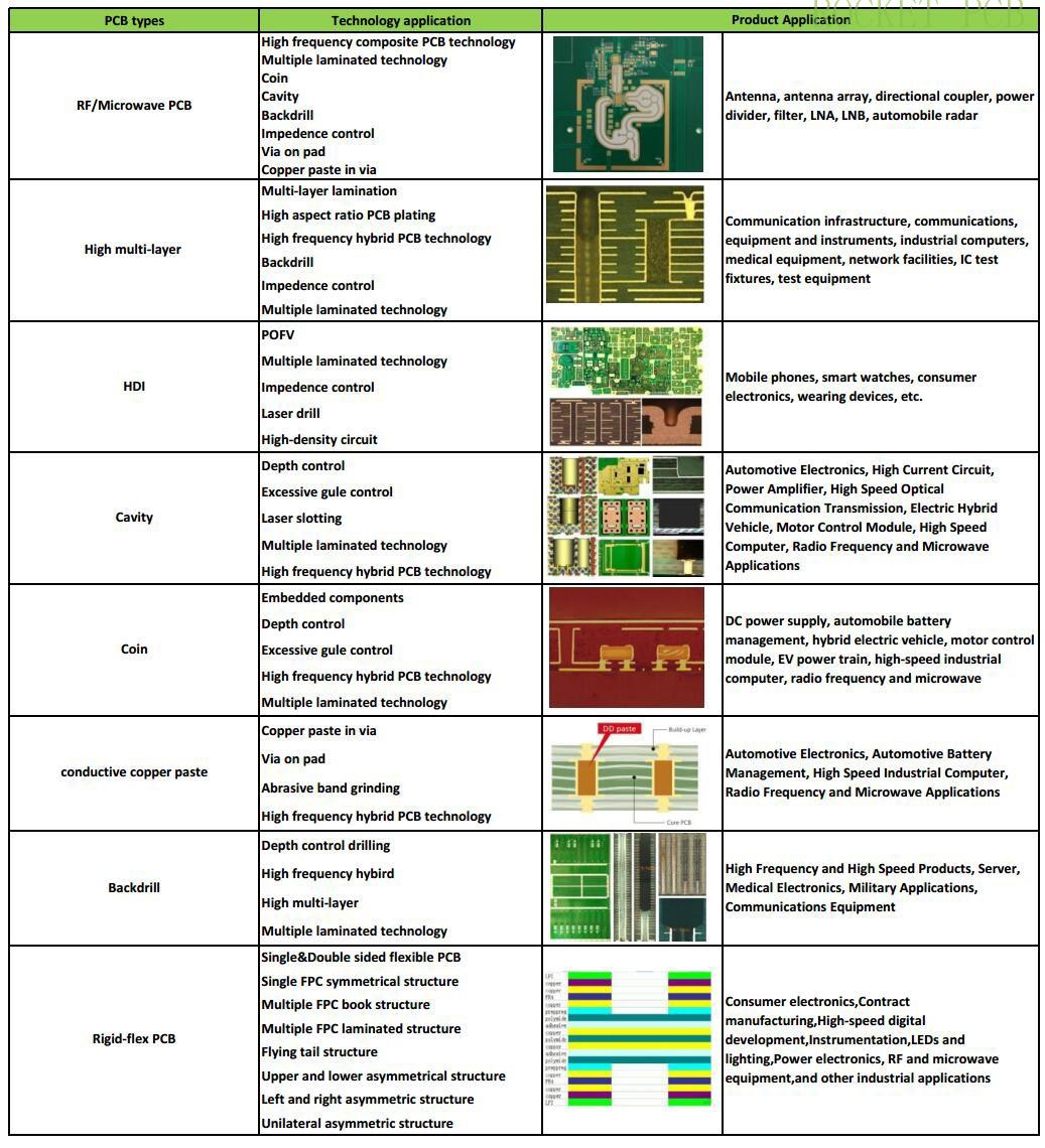
See our competency PCB capabilities table.
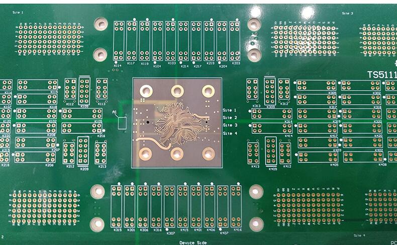
HDI PCB manufacturing is the core manufacturing service of Rocket PCB, which has various functions and can meet the most demanding requirements of HDI PCB manufacturing. Our strong PCB manufacturing capabilities can meet the stringent requirements of all industries (including medical, aerospace, defense, and commercial markets) for advanced HDI PCB design.
We support up to 40 laminates, laser drilling, micro through holes, stacked micro through holes, blind holes, embedded through holes, through holes in pads, laser direct imaging, sequential lamination, etc. 00275 "trace/spacing, fine pitch as low as 3mil, controllable impedance, etc.
We produce HDI PCB without minimum order requirements and flexible turnaround time options.
Prior to production, our CAM engineers will review each design in detail to ensure that they are not worried about the manufacturing process, and the support team will provide you with HDI PCB manufacturing orders 24 hours a week from Monday to Sunday.
The difficulty of the HDI PCB board lies in micro hole manufacturing and through-hole metallization, which puts forward higher requirements for electroplating capacity of the production line, so VCP plating is often used, and the design of HDI fine circuit requires direct imaging equipment of LDI. For example, 4 + N + 4 multi-laminate structure has more advanced requirements for the accuracy of laminating equipment and the ability of process level.
HDI manufacturers need more advanced equipment and more investment. Only years of HDI production experience can guarantee the quality of the HDI board. Rocket PCB is good at this, and its HDI board is widely used in many fields, such as medical, aerospace, national defense, and commercial market.
High-frequency PCB is mainly used in the communication industry. The development of 5G technology provides a good opportunity for high-frequency PCB manufacturing. It is a new growth point for domestic high frequency board manufacturers. However, there are also disadvantages, that is, high-frequency material is not easy to obtain, the manufacturing maturity of unconventional high-frequency material is not high, and the process control is not in place, resulting in the production of boards can not fully meet the requirements of high-frequency signal transmission. So the domestic manufacturers who are good at high frequency board manufacturing are few.
On the one hand, large factories can give priority to obtaining HF materials and obtaining the priority of high-frequency material suppliers. After signing the agreement, the plates can be purchased for production in time. Some manufacturers need a long procurement cycle to purchase high-frequency materials.
On the other hand, the production and manufacturing of high-frequency PCBs are quite different from that of the ordinary board. In addition to the requirements of conventional dielectric constant and TG, the adhesion of high-frequency materials to copper plating is not high, which needs to be roughened by plasma equipment. The tolerance of the impedance signal line is very strict. The process also requires higher-level parameters.
Because of the special material, there is more burr in milling, so a special milling cutter is needed.
High-frequency PCB is widely used in mobile communication products and intelligent lighting system
Power amplifier, low noise amplifier, etc
Power divider, coupler, duplexer, filter, and other passive components
In the field of automotive collision avoidance system, satellite system, and radio system
Generally speaking, high frequency PCB materials include ro4350b, ro4003c, ro3010, and rt5880. In addition, there are other high-frequency materials, such as Taconic high-frequency material, PTFE high-frequency board, Arlon, Isola material, and so on.
Rocket PCB is a professional high-frequency PCB manufacturer. Rogers high-frequency PCB prototype production is more completed on the high-frequency board. In the high-frequency material inventory, multiple models and types of high-frequency boards respond quickly and timely. Some materials need to be purchased in advance, and you should be informed in time. We will arrange orders for you in time. If you are looking for high frequency PCB, we can help you find the right substrate, determine the width and spacing of conductors, calculate the impedance, etc.
Due to the characteristics of copper thick (≥ 3oz) thick copper PCB, there are many processing difficulties in the PCB production process, especially in the laminating process, after the large copper-free area is laminated, it is easy to appear cavity and uneven thickness. This is in the graphic design, PP selection, laminating program matching, laminating machine temperature rise and vacuum capacity, and the solution of inner layer glue (flow glue route), residual copper rate control, withstand voltage requirements, key points of thick copper PCB project, circuit coil treatment, multiple electroplating, multiple solder resistance, etc. are accumulated experience, so it has a certain technical threshold. Rocket PCB has rich experience in providing prototype design and processing services for thick copper PCB.
Thick copper PCB has many advantages,
Increased resistance to thermal stress
The current carrying capacity increases
Increased connector position and mechanical strength in PTH holes
Make full use of exotic materials to achieve their full potential (i. e. high temperature) without circuit failure
Reduce product size by combining multiple copper weights on the same circuit layer
Heavy copper plated vias flow higher current through the plate and help transfer heat to the external radiator
The on-board radiator is directly plated onto the plate surface with up to 120 ounces of copper
Onboard high power density planar transformer
The traditional radiator assembly process involves three labor-intensive and expensive steps. The time and work required to complete this process are very time-consuming, and the result is not as good as the mechanical automation process. On the contrary, the built-in radiator is produced during the PCB manufacturing process and no additional assembly is required. Heavy-duty copper circuit technology makes this possible. The radiator is plated on the surface, so it is connected to the heat-conducting through-hole without any interface hindering heat conduction. Another advantage is the addition of a copper coating in the cooling holes, which reduces the thermal resistance of the circuit board design because planar windings are actually flat conductive traces formed on the copper-clad laminate, so they can improve the overall current density compared to cylindrical wires. This benefit is due to the minimization of the skin effect and higher current carrying efficiency.
When making heavy copper circuits, we usually have to deal with a large number of plating thicknesses. Therefore, allowance must be made in defining the wire spacing and pad size. Therefore, it is suggested that designers should include PCB manufacturers in the early stage of the design process.
There are many names for these products; Aluminum clad, aluminum base, Metal clad printed Circuit Board (MCPCB), Insulated Metal Substrate(IMS or IMPCB), Thermally conductive PCBs, etc… but they all mean the same thing and perform the same way.
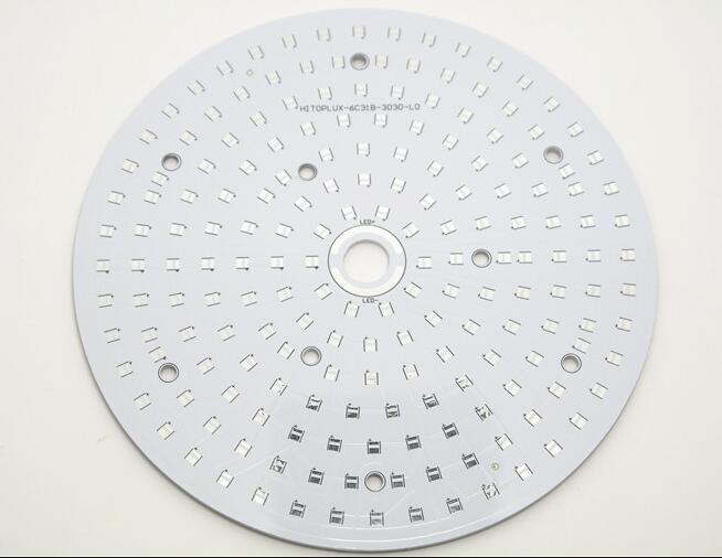
Rocket PCB produces aluminum printed circuit boards (PCBs), whose materials from leading global suppliers, offering a wide range of high-performance and low-cost materials. The aluminum pcb, which consists of a dielectric metal substrate and a bonded copper circuit layer, produces excellent heat transfer, which helps cool components while eliminating problems associated with managing fragile ceramics.
Rocket PCB is committed to becoming the best aluminum PCB manufacturer. We provide a variety of conductive and thermal interface pads, thermal gap fillers, thermal phase change materials.
Key requirements for selecting aluminum PCB manufacturers
In most cases, PCB manufacturing follows the same production process no matter where it is produced. The only real difference between suppliers is the level of automation of the process, the latest technology and equipment, and having specific equipment specifically for certain types of end products. For aluminum pcb, if PCB manufacturers want to be able to effectively produce any number of aluminum PCB, several key items need to be considered, including:
Special imaging equipment
Many of our aluminum based PCBs take longer to enter LED applications than standard 18 "x 24" or 20 "x 24" production panels used in traditional PCB manufacturing. To be able to accurately register and economically produce these parts, the manufacturer must have a custom-made 60 inch wide UV imaging device, or a setup that can screen print (once) images and then UV cure them through the oven.
Professional V-CUT equipment
More common devices that can obtain V scores from traditional FR-4 materials are not suitable for managing aluminum PCBs. In order to get the lowest cost, we need to get the best yield, which means we need to be able to place these parts as close to each other as possible on the production panel. If there is no V score, the parts must be mechanically ground, which can result in a yield loss of up to 20%, thereby increasing costs.
Our engineering team has many years of experience to help our customers design the cheapest array.
Punch
For circular or aluminum pcb with unique features (slots, large holes, notches, etc. ), you need the aluminum PCB manufacturer to be able to provide these features. Mechanical grinding of aluminum PCB is a very expensive method to complete these functions in the production environment. Advanced die is required for stamping forming, with neat edges and no burr.
High voltage test
The unique requirement of aluminum PCB is that customers want to know that the products obtained have passed the withstand voltage test. Although most PCB manufacturers can do this, it is usually a separate process in the laboratory, and we provide free electrical testing to our customers.
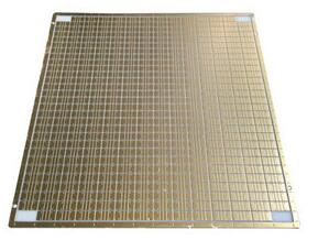
Backplane PCB, also known as motherboard, is a kind of substrate, which is responsible for carrying function board, including daughter board or line card. The main task of the backplane is to carry the daughter board and distribute the power to the function board to realize the electrical connection and signal transmission. The backplane PCB is a high-end product in the industry. Because of the super high-rise number, super large size, back drilling and deep drilling control, the factory can complete it as long as it has the strength of large equipment.
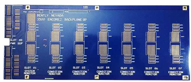
The unique features of the backplane include,
Size
A large part of the backplane is connected at right angles to some other boards. This requires the backplane to be much larger than the traditional PCB, and some backplanes can even reach 762mmx1066. 8mm
Number of layers
For the most common backplane, the number of layers is between 16 and 28, which is much higher than that of ordinary PCB
Thickness
From the structure of the base board itself, in order to withstand greater mechanical stress, it must be designed to be much thicker than ordinary PCB. In most cases, the designer must increase the thickness. The typical thickness of the backplane board is 2mm-4mm, which can be up to 4mm-6mm.
In order to achieve such high-performance requirements, PCB manufacturing must face the challenges of strict board thickness, board size, number of layers, alignment control, back drilling depth and short line.
Rocket PCB provides powerful resources for the production of back drilling PCB. Our board factory is the world-class level and is the industry leader. Rich experience in back drilling PCB board processing, reliability certified by a large number of customers. If you have back drilling PCB/backplane PCB processing requirements, please consult us.
Ceramic PCB / ceramic substrate is a special process board. Copper foil is directly bonded to the surface of alumina (Al2O3) or aluminum nitride (AlN) ceramic substrate (single or double sided) at high temperature. The ultra-thin composite substrate has excellent electrical insulation, high thermal conductivity, excellent solderability and high adhesion strength. It can etch all kinds of patterns and has a great current carrying capacity. Therefore, the ceramic substrate has become the basic material of high-power electronic circuit structure technology and interconnection technology.
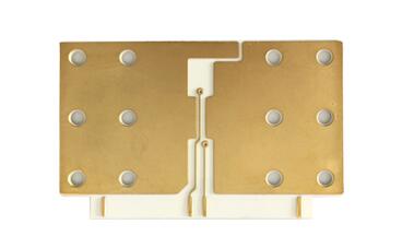
Ceramic PCB application
High power semiconductor module; semiconductor cooler, electronic heater; power control circuit, power mixing circuit.
Intelligent power module, high frequency switching power supply, solid-state relay.
Automotive electronics, aerospace and military electronic components.
Solar panel module; telecommunication special exchange, receiving system; laser and other industrial electronics.
The birth and development of FPC and PCB gave birth to the new product of a rigid-flex board. Therefore, the rigid-flex PCB is a PCB with FPC characteristics and PCB characteristics formed by combining flexible PCB and rigid PCB and through pressing and other processes according to relevant process requirements.
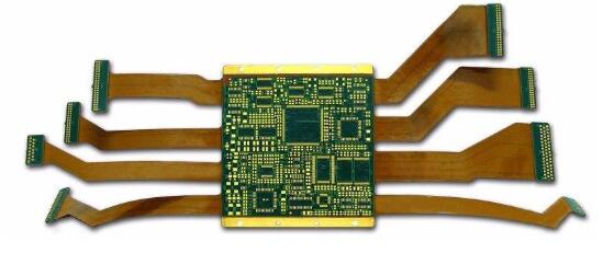
Rigid-flex design is more challenging than a typical rigid PCB environment because these panels are designed in 3D space, which also provides higher spatial efficiency. By being able to design in three dimensions, the rigid-flex PCB designer can twist, fold, and roll up the flexible board substrate to achieve the shape required for the final application packaging.
Compared with the manufacturing of rigid boards, the development of rigid-flexible PCBs involves a more complex and time-consuming manufacturing process. Compared with the rigid FR4 PCB, the treatment, etching, and soldering process of all flexible components of the rigid-flex board are completely different.
According to different applications, complete rigid-flex PCB can be manufactured symmetrically with internal flexible boards or unsymmetrically with external flexible boards. there are various circuit designs available.
In the early stage of PCB design, serious consideration of rigid-flexible solutions and appropriate evaluation of available options will yield significant benefits. It is crucial that PCB manufacturers be involved early in the design process to ensure that the design and Fab parts are consistent and that differences in the final product are taken into account.
QUICK LINKS
CONTACT US
Office: (+86) 755 23040566
Tel: (+86) 158 9965 5195
E-mail: sales@rocket-pcb.com
Skype: Hans@Rocket-PCB
Whatsapp: 86 1589965 5195
Office Address: 2207,Bid 4,He Gu Shan Hui Cheng,35#,Guang Tian RoYanluo street, Song Gang Town,518105 SHENZHENG, CHINA
Plant ADD.: No 69, Lianfeng North Road, Xianxi Area, ChangAn Town, Dongguan, China.


