


What are the types of PCB drilling in PCB production
PCB drilling is a very important process in PCB manufacturing process, it has three common drilling methods, namely through hole, blind hole and buried hole. Today we will introduce their meaning and characteristics.
Through hole
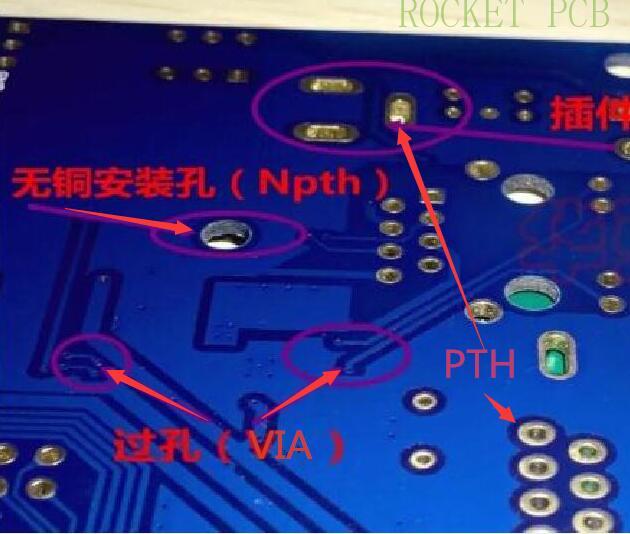
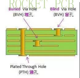
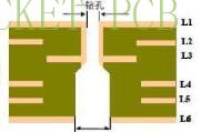
Through hole is also known as PTH, the abbreviation of plating through hole. It is the general name of through-hole plug-in components in electronic industry, including dip, PICC, PTH, etc. The metal tube passes through the hole of the circuit board, and the copper surface is connected with the top and bottom circuit of the double-sided board, which also plays the role of connecting the inner layer in the multilayer board. Due to the large diameter of PTH hole, the production cost is relatively cheap. The disadvantage is that it takes up a lot of effective space. A large number of through holes cause great obstacles to the wiring of the inner layer of multi-layer PCB. These through holes occupy the space required for wiring. They pass through the surface of power supply and ground wire layer intensively, which will destroy the impedance characteristics of power ground layer and make the power ground layer invalid.
Via hole
Via hole (VIA) is a through hole, but the hole diameter is small, is used to conduct or connect copper foil circuits between conductive patterns in different layers of a circuit board. For example (such as blind hole, buried hole), but can not insert component leg or other reinforcement of copper plated hole. Because PCB is formed by stacking and accumulating many copper foil layers, a layer of insulation layer is laid between each layer of copper foil, so that the copper foil layers cannot communicate with each other, and the signal connection depends on via.
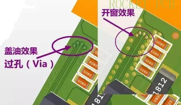
The feature is: in order to meet the needs of customers, the via hole of circuit board should be plugged. In this way, in the process of changing the traditional aluminum sheet plug hole technology, the white mesh is used to complete the solder mask and plug hole on the circuit board surface, so that the production is stable, the quality is reliable, and the application is more perfect. With the rapid development of electronic industry, higher requirements are put forward for the process and surface mounting technology of printed circuit board. Via hole plug hole technology on the application was born, there are generally the following three different requirements
1. Copper can be in the via hole, solder mask ink can be plugged or not be plugged.
2. There must be tin and lead in the through hole. If there is a certain thickness requirement (4um), no soldermask ink is allowed to enter the hole, resulting in tin beads hidden in the hole.
3. Via hole must have solder resist ink plug hole, opaque, no tin ring, solder bead and leveling requirements.
Via (via) is one of the most important parts of PCB, which is the electrical connection guide hole between layers. It is made by electroless copper process.( Copper deposition). The cost of drilling usually accounts for 30% to 40% of the cost of PCB making. Therefore, when drawing PCB board, the inner diameter of via hole should be greater than 0. 25 mm, and the outer diameter should be greater than 0. 4 mm, otherwise the manufacturing cost of PCB will be increased.

Blind hole
Blind hole: is to connect the outermost circuit in PCB with the adjacent inner layer by electroplating hole, because the opposite side cannot be seen, it is called blind hole. At the same time, in order to increase the space utilization between PCB layers, blind holes are applied. That is, a via hole to one surface of the printed board.
In PCB design, although the size of pad and via has been gradually reduced, if the thickness of the board does not decrease proportionally, the aspect ratio of through-hole will increase, and the increase of aspect ratio of through-hole will lead to insufficient copper deposition in the hole, thus reducing the product reliability. With the development of advanced laser drilling technology and plasma dry etching technology, small aperture blind holes and buried holes emerge as the times require. If the non conducting aperture is 0. 3mm, the parasitic parameters will be about 1 / 10 of the original conventional holes, which improves the reliability of PCB. In PCB production, special attention should be paid to the drilling depth (Z-axis), otherwise it will cause difficulties in electroplating in the hole. The circuit layer that needs to be connected can be drilled in advance in individual circuit layer, and then pressed. It needs more precise positioning and alignment device.
Buried hole
Buried hole refers to the connection between any circuit layers in PCB, but it does not conduct to the outer layer, and it also means that the through hole does not extend to the surface of the circuit board.
Features: in this process, it is impossible to drill holes after bonding. Drilling must be performed at the time of individual circuit layers. First, the inner layer is partially bonded and then electroplated. Finally, all the bonding can be achieved. It takes more time than the original through-hole and blind hole, so the price is also the most expensive. This process is usually only used for high density circuit boards to increase the usable space of other circuit layers.
The buried hole is the connection of any circuit layer in PCB, but it is not connected to the outer layer. Due to the use of non-conductive perforation technology, there are few large via holes on PCB, thus providing more space for wiring. The remaining space can be used for large area shielding to improve EMI / RFI performance. At the same time, more space can also be used for the inner layer to partially shield the device and the key network cable, so that it has the best electrical performance. The use of non-conductive holes makes it more convenient to fan out the device pins, which makes the wiring of high-density pin devices such as BGA packaging devices easy, shortens the connection length, and meets the timing requirements of high-speed circuits.
Depending on the function of the hole, there are other types of holes,
Depth control hole
Depth control hole is to control a certain depth without drilling through the circuit board. There are many kinds of depth control holes, which are usually drilled with a certain depth by controlling the drilling height of the main shaft. There are similar mechanical blind holes, back drills, and some are depth controlled gongs, with similar mechanisms.

Counterbore
The hole where the head of the fastener is partially or completely sunk into PCB is called countersunk hole. PCB's countersunk hole is mainly used to make the circuit board's layers connect and fix parts. PCB has strict requirements on the depth and size of countersunk hole, and its size should be limited within the tolerance range
Back drilling hole
PCB back drilling is a kind of hole which can control the depth by mechanical drilling, remove the copper part of the PTH hole that does not need to be conducted and will interfere with the signal, and retains the hole copper needed for conducting. The design principle of back drilling: analyze the characteristics of signal transmission from the angle of hole. If the through-hole is designed, the loop signal transmission will bypass. The existence of this section of through-hole will easily cause problems such as reflection and scattering of signal transmission, resulting in signal disturbance and distortion. When the extra hole copper is drilled, the signal will return according to the original path. At this time, the inductance generated by the removed signal can be offset and the signal distortion can be minimized.
PCB crimping hole
PCB crimping hole refers to those holes which can be fixed directly by inserting components without welding. The aperture tolerance is more strict than the general aperture tolerance. The conventional crimp hole tolerance is + / - 0 . 05mm, some of which can even reach + / -0. 025mm. However, the crimping holes are mostly standard PIN components.
In PCB production, drilling this item is very important, can not be careless. Drilling is to drill the required through-hole, so as to connect components and play a fixed function. If there is a problem with the via hole, the device can not be fixed on the board well. The use of the board is affected at the slightest, while the whole board will be scrapped, so the process of drilling is very important.


