


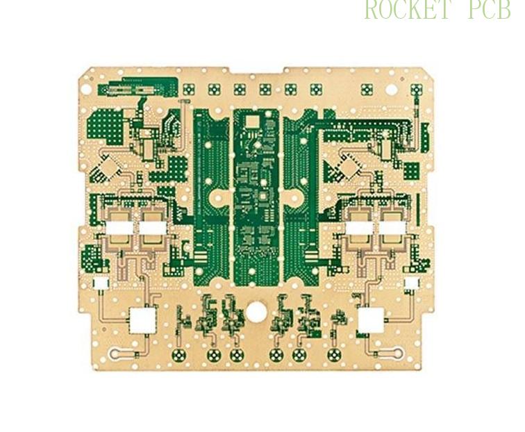
High Frequency PCB In The Electronics Manufacturing Industry
Introduction
The engineering world is equipped with installing high frequency PCBs in different devices. Their exceptional properties and high-end performance are outstanding and offer to be an integral part of various electronic devices used worldwide.
There are many important details regarding high frequency PCB that you might be interested in knowing, so let's have a look at this article below:
What is high frequency PCB?
The high frequency PCB works with the mechanisms where electromagnetic waves are transmitted, and it is even used in such devices where signal transmission is needed. Fabricating a high frequency PCB is a technical one, and unique materials are required for the purpose.
The signals from this kind of PCB flow at a very high rate, and the frequency amounts to be around 100 GHz. The common use of these boards is found mainly in HDI technology, as the transmission of signals needs to be optimal in these devices.
What is a high-speed digital design?
A high-speed digital design comprises various factors that need to be considered to ensure that the optimal transmission of the signals is achieved. Multiple considerations are also needed in the PCBs comprising high-speed ones, and some of the essential aspects of such designs include the following:
● Low dissipation is one of the factors that is the reason for the high speed of signals. Due to this low dissipation, the signal loss is less; hence, the transition is quite strong. In the case of such designs, the optimal dissipation rate ranges somewhere between 0.0019 to 0.025.
● The dielectric constant in these designs is low, and when it comes to this aspect of the design in high frequency PCB, the best part is that there are no delays in the transmission of the signal, and the job is done fast.
● Resisting the chemical reactions is also one of the most important aspects of the high frequency PCB that helps protect the boards from corrosion.
● It is imperative for PCBs to withstand conditions of moisture and with the high frequency PCB.
Designing high frequency PCBs requires attention
The process of designing a high frequency PCB is a technical one, and while designing it, specific guidelines must be followed:
Impedance
It is imperative to have controlled impedance. If the meaning of the environment is done carefully, the impedance control will be recovered. When it comes to high frequency PCB, the behavior of the circuit traces is complex.
By way of controlled impedance, there is a surety that the signals won't be subjected to any degrading as they move around the PCB.
Component Location
The location of the components is another essential aspect that must be addressed. It is imperative to divide the PCB ground into areas where different components and connections will be placed. Location accuracy also plays an essential role in high frequency PCBs because it helps develop the correct circuit route for signal transmission.
Crosstalk
Crosstalk is the issue that arises when signals tend to get in contact with one another, creating a distortion. This must be avoided at all costs. The traces need to be planned and placed on the PCB to be relevant with distance.
Also, the components must be placed perpendicular to one another, as this will help avoid crosstalk. The objects that have their signals transmitted must be kept away from the ground plane, such as the clocks so that no crosstalk appears between the two signals.
Signal Integrity
Devising a route for signals where the two different signals do not interact is also very important. Hence the digital signals and the analog signals, both must be routed differently. If they come into contact with each other, there is a high chance that the PCB will lack signal integrity.
High-Speed Routing
The width spacing in the routes is a prime concern in the high frequency PCB; hence, it must be taken care of. The channels created for the circuits for signal routes must have the proper width spacing between individual traces and the traces of net groups.
Power Integrity
The network of delivery for the voltage in the circuit board is essential. The power must be stable and provided to all the components correctly. Hence, as much as the layout is necessary, it is crucial to ensure that the power is distributed evenly across the PCB.
High frequency PCB characteristics
There are various characteristics associated with the high frequency PCB; some of these characteristics include the following:
● High frequency PCB manages heat dissipation very well and doesn't let the component get heated up during the function.
● The performance of this kind of PCB is excellent, and it doesn't cause any signal loss during the process; hence the signal strength is maintained.
● It doesn't absorb water, so the moisture rate of this kind of PCB is also significantly less.
● High frequency PCB is a highly stable form of PCB in mechanical terms.
High frequency PCB manufacturing process
The following process is followed when it comes to manufacturing a high frequency PCB.
● The first step of manufacturing a high frequency PCB is to plan the board's design to determine where each component will be placed.
● The design is then oriented with the plotter, giving a clear print of the conductive and the non-conductive areas.
● The design of the PCB is printed on the laminate, and then on the same laminate, the copper is bonded.
● The next step is to align the layers and press them into the board to remain intact.
● Drilling the board is the next step, where with the help of an x-ray machine, the holes are marked and then drilled.
● Chemical is then used to join each layer so that the next stage of soldering can be undertaken, where a solder mask is applied to the board and then exposed to the UV rays.
● The unwanted parts of the solder mask are removed with the UV light, and then the plating is done, followed by printing the details.
● Testing is also critical, in which the connections are tested to ensure no short connections.
● Lastly, a CNC machine cuts the board down in the required shape.
Applications of high frequency PCBs
There are various applications of the high frequency PCBs and some of the compromises of the following:
● In the communication sector, high frequency PCBs are common and mainly used in amplifiers, boosters, receivers, etc.
● The manufacturing of military weapons also consists of using high frequency PCB.
● The latest medical equipment used for diagnosis purposes is also backed with high frequency PCBs.
Conclusion
At Rocket PCB, a comprehensive option of PCBs manufactured for various electronic devices exists. Similarly, the high frequency PCB is also one of the kinds which are manufactured. You can always have your appliances backed without PCBs, and you will be satisfied. So, get in touch with us, and we will gladly assist you.


