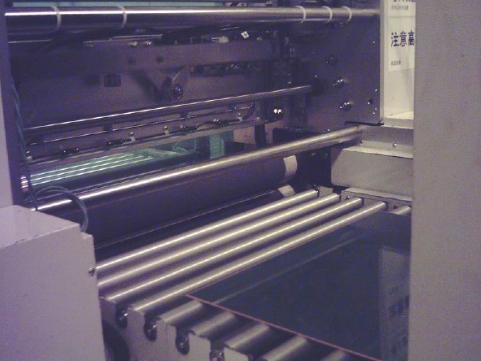
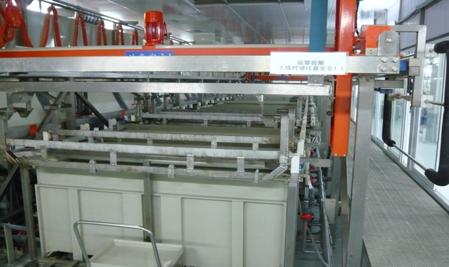
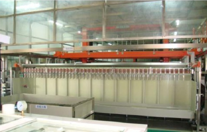
Multilayer PCB Lamination
The control of lamination quality is becoming more and more important in multilayer PCB fabrication. Therefore, it is necessary to ensure multilayer laminate quality, need to have a good understanding of multilayer laminate technology. According to the processing practice for many years, Rocket PCB summarizes how to improve the laminating quality of multilayer boards as follows,
1. The thickness of the core board should be selected according to the total thickness requirements of the multilayer board. The thickness of the core board should be consistent and the deviation is small.
2. There should be a certain distance between the overall dimension of the core board and the effects unit, that is, the distance from the effective unit to the edge of the board should be on the premise of not wasting materials try to keep more space.
3. Design of positioning hole. In order to reduce the deviation between layers, attention should be paid to the design of positioning holes in multi-layer boards: 4-layer multilayer only needs to be designed more than 3 positioning holes can be used for drilling. For multi-layer boards with more than 6 layers, in addition to designing positioning holes for drilling, it is also necessary to design more than 5 overlapping positioning rivet holes and more than 5 positioning holes for the tool plate for rivets.
4. The inner core board shall be free from the open, short, open circuit, oxidation, clean board surface, and no residual film.
5. Meet the requirements of PCB users, select the appropriate PP and copper foil configuration. For 4-ply laminates, 7628, 7630 or 7628 + 1080, 7628 + 2116 can be used etc. 1080 or 2116 is the main choice of PP for multilayer boards with more than 6 layers, and 7628 is mainly used to increase the thickness of the dielectric layer. At the same time, PP requires symmetrical placement to ensure mirror effect and prevent plate bending.
6. Inner core board pretreatment process. The treatment process of the inner layer core board includes the black oxidation process and browning treatment process. The oxidation treatment process is to form a black oxide film on the inner copper foil, the thickness of the black oxide film is 0.25-4.50mg/cm2. The browning process (horizontal browning) is to form an organic film on the inner copper foil.
The functions of the inner laminate treatment process are as follows:
a. Increasing the surface ratio of inner copper foil and resin can enhance the adhesion between them.
b. The effective wettability of the melt resin to copper foil is increased so that the flowing resin has sufficient ability to penetrate into the oxide film and show a strong grip after curing.
c. It can prevent the decomposition of dicyandiamide in liquid resin at high temperatures and influence on the copper surface.
d. It can improve the acid resistance and prevent the PINK ring in the wet process.
7. The organic matching of lamination parameters, the control of multi-layer board lamination parameters mainly refers to the organic matching of lamination "temperature, pressure, and time". How to determine the lamination temperature, pressure, and time software parameters is the key technology for multilayer laminate processing.
Materials for making multilayer PCB
Copper foil
Basic material composed of the conductive pattern
Core board
A framework of the circuit board, double-sided copper clad board, which can be used for double-sided board production.
Prepreg
The indispensable material for multilayer board production and the adhesive between core board and core board plays an insulating
role at the same time.
Various types of most commonly used FR-4 prepreg materials
Material name | Material type | Original thickness (um) |
FR4 | 7628 | 193 |
2116 | 122 |
3313 | 99 |
1080 | 74 |
How to make multilayer PCB?
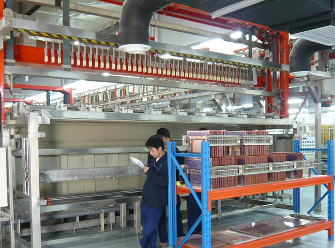
Multilayer PCB flow-Main processes
Inner Layer Pre-processing
The purpose of the plating process is to thicken the copper thickness in the hole to prevent the hole copper from being insufficient and causing micro corrosion. The copper thickness in all holes of the working panel is 5 ~ 10 um, and the surface copper thickness is increased by 5 ~ 10 um
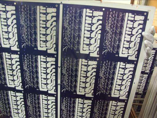
Pattern transfer----Exposure---Develop ( Same as inner layer process)
Difference between single layer and multilayer PCB
Compared with a double-layer board, the multilayer PCB has greatly improved electromagnetic compatibility.
For example, in a four-layer board, the middle layer is used as a power layer and a ground layer, and the benefits of doing so are as follows,
1. The inductance of the power wire and ground wire is greatly reduced, thus reducing the noise voltage
2. The power supply layer and ground layer form a large distributed capacitor, which provides a good high-frequency decoupling effect for the power supply, thus reducing the noise on the power cord.
3. Independent power and ground layer can minimize the area of all signal loops
4. PCB multilayer board is the trend of the circuit board industry, the circuit board industry is developing toward a smaller size, the smaller the hole, the thinner the thickness, the larger the number of layers, the smaller the line width and spacing, and so on.
5. Many high-precision high-tech electronic products are required multilayer PCB boards to achieve functions, the ordinary double-sided board simply cannot replace them.
Types of multilayer boards
According to usage, it can be divided into
Civil printed circuit board (consumer electronics such as TV sets, electronic toys, etc. )
Industrial printed boards (computers, instruments, etc. )
Printed circuit board for military & Aerospace
According to hardness, it can be divided into
According to the conduction state of the hole, it can be divided into
Classification by substrate
Application of Multilayer PCB
As mentioned above, multilayer PCB can be used in civil, industrial, and military fields. Multilayer PCB can be used for any purpose.
For many industries, multilayer PCB has become the first choice for various applications. This preference is largely due to the continuous promotion of mobility and functionality by all technologies. Multilayer PCB is a reasonable step in this process, which can reduce the size and realize more functions. As a result, they have become quite common, including:
Consumer electronics: consumer electronics is a broad term, such as smartphones and microwave ovens. Each of these consumer electronics products contains PCB, but more and more of them use multilayer PCB instead of standard single-layer PCB, which is used to increase function and reduce size.
Computer electronics: everything from the server to the motherboard uses multilayer PCBs, mainly because of their space-saving and high functionality. For these applications, performance is one of the most basic characteristics of PCB.
Telecommunications: telecommunications equipment typically uses multilayer PCBs in a variety of general applications, such as signal transmission, GPS, and satellite applications. The main reason is its durability and functionality.
Industrial: Multilayer PCB has become popular in several industrial applications, the most notable of which is industrial control. From industrial computers to control systems, multilayer PCBs are used to run machines throughout manufacturing and industrial applications, contributing to their durability and small size.
Medical devices: electronic products are becoming an increasingly important part of the healthcare industry, playing a role in every corner of the industry, from treatment to diagnosis. Compared with single-layer substitutes, multilayer PCB is particularly popular in the medical industry because of its small size, lightweight and powerful functions. These advantages make multilayer PCB used in modern X-ray equipment, cardiac monitor, CAT scanning equipment, and medical test equipment.
Military and national defense: multilayer PCBs are favored in terms of durability, functionality, and low weight, and are very useful in high-speed circuits, which are getting more and more attention in military applications. As the defense industry moves towards highly compact engineering, they are also favored, as smaller multi-layer PCBs leave more space for other components to perform their existing functions.
Automobile: in the modern automobile, the automobile is more and more dependent on electronic components, especially with the rise of an electric vehicles. From GPS and onboard computers to headlight switches and engine sensors controlled by electronic devices, using the right type of components is becoming increasingly important in vehicle design. Multilayer PCB has high function and relative heat resistance, so it is very suitable for the interior environment of automobiles.
Aerospace: like cars, jets, and rockets, they rely heavily on modern electronics, all of which have to be very precise. From the computer used on the ground to the computer used in the cockpit, the application of aerospace PCB must be reliable. In this case, multilayer PCB is the ideal solution, with enough protection layer to keep heat and external stress from damaging the connection, and the ability to be made of flexible materials. Their higher quality and functionality also contribute to this utility in the aerospace industry, as aerospace companies prefer to use the best materials to ensure the safety of personnel and equipment.
There are more! Multilayer PCB is used in a variety of other industries, including the science and research industry, even household appliances and safety. All devices, from alarm systems and optical fiber sensors to atomic accelerators and weather analysis equipment, use multilayer PCBs, making full use of the space and weight saved by this PCB format.
Rocket PCB Solution Ltd is widely known as a professional PCB supplier in the electronic manufacturing industry. We have years of experience in the multilayer PCB, HDI PCB segments. Rocket PCB further expands its range of products including rigid, rigid-flex, HDI, any layer, Flex, large-size, embedded, RF, LED, backplane, the metal substrate, a ceramic substrate, IC structure, high-frequency, heavy copper. High quality and high reliability.
Get Fast Quotation
How to design multilayer PCB
In designing Multilayer PCB, one of the most important things is to plan the stack of Multilayer PCB to achieve the best performance of the product. The bad design of the substrate and improper selection of materials will reduce the electrical performance of the signal transmission, increase emission and crosstalk, and make the product more vulnerable to external noise. These problems can lead to intermittent operation because timing glitches and interference can significantly reduce product performance and long-term reliability.
Multilayer PCB stack
In contrast, a properly constructed PCB board can effectively reduce electromagnetic radiation, crosstalk and improve signal integrity, thus providing a low inductance distribution network.
According to experience, compared with a double-sided PCB board, the radiation of a four-layer board will be reduced by 15 dB.
When selecting a multilayer stack, we should consider the following factors:
1) Below the surface of the component (the second layer) is the ground plane, which provides the components shielding layer and provides the reference plane for the component surface wiring;
2) All signal layers shall be adjacent to the ground plane as far as possible;
3) Try to avoid two signal layers directly adjacent;
4) The main power supply should be adjacent to its corresponding ground as far as possible;
5) In principle, a symmetrical structure design should be adopted. The meaning of symmetry includes: thickness and type of dielectric layer, the thickness of copper foil, and figure
6) The distribution type (large copper foil layer, circuit layer) is symmetrical.
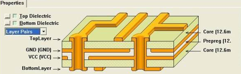
Let's take a look at the most common multilayer PCB Lamination
4 Layer PCB lamination
A typical four layers PCB laminate is shown below.
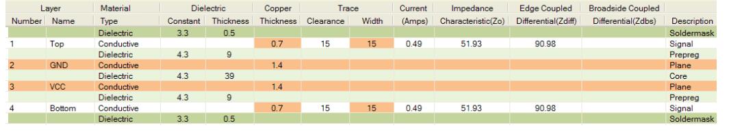
4 Layer PCB stack
Four layers of PCB are usually seen stacked evenly. That is, four evenly spaced layers with the plane at the center. While this does make the board symmetrical, it does not help EMC.
In addition, another common mistake is to make the plane tightly coupled to the large dielectric layer and plane between the center and the signal. This certainly produces good interplane capacitance, but it also doesn’t help signal integrity, crosstalk or EMC – that’s why we chose to use 4-layer PCBs on two layers.
To improve the EMC performance of the capacitor, it is better to put the signal layer as close as possible to the plane (< 10 mil), and use a large core (~ 40 mil) between the power supply and the ground plane to maintain the overall substrate thickness 62 mil. Close tracking of planar coupling will reduce crosstalk between traces and allow us to keep impedance at an acceptable value.
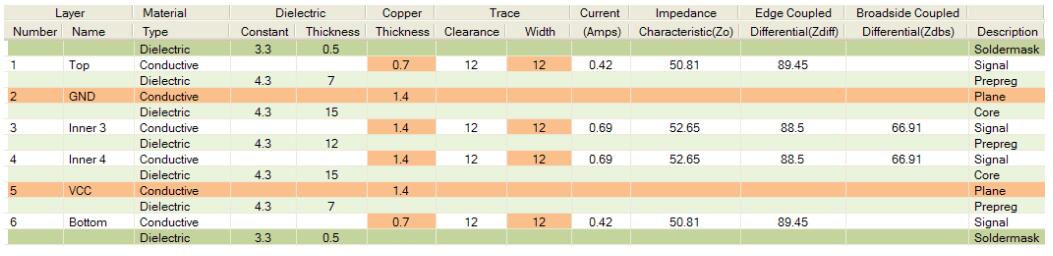
6 Layer PCB stack
The six-layer PCB board is basically a four-layer board, adding two additional signal layers between the planes. This greatly improves EMI because it provides two buried layers for high-speed signals and two surface layers for routing low-speed signals. The signal layer should be placed very close to the adjacent plane and the plate thickness (62 mil) should be composed of a thicker central core. There is always a trade-off between trace impedance, trace width and prepreg/core thickness. Differential pairs are becoming more and more common in high-speed design. Noise is reduced by using differential mode signals.
6 Layer PCB stack& 8 Layer PCB stack
To improve EMC performance, add two more planes in the six stack. It is recommended not to have more than two adjacent signal layers between the planes as this creates impedance discontinuities (signal layer impedance difference of ~ 20 Ohm) and increases crosstalk between these signal layers.
In the following case, two plane layers are added to the center of the substrate. This allows tight coupling between the central planes and isolates each signal plane, thereby reducing coupling and significantly increasing crosstalk. This configuration is usually used for high-speed signals in DDR2 and DDR3 designs where crosstalk due to tight wiring is a problem.
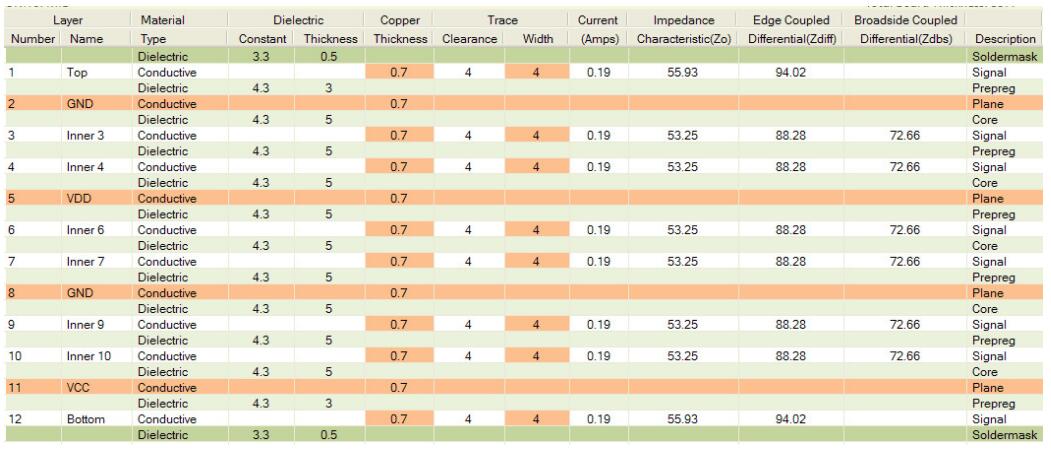
10 Layer PCB stack
When six wiring layers and four planes are required, ten layer boards should be used - and EMC deserves attention.
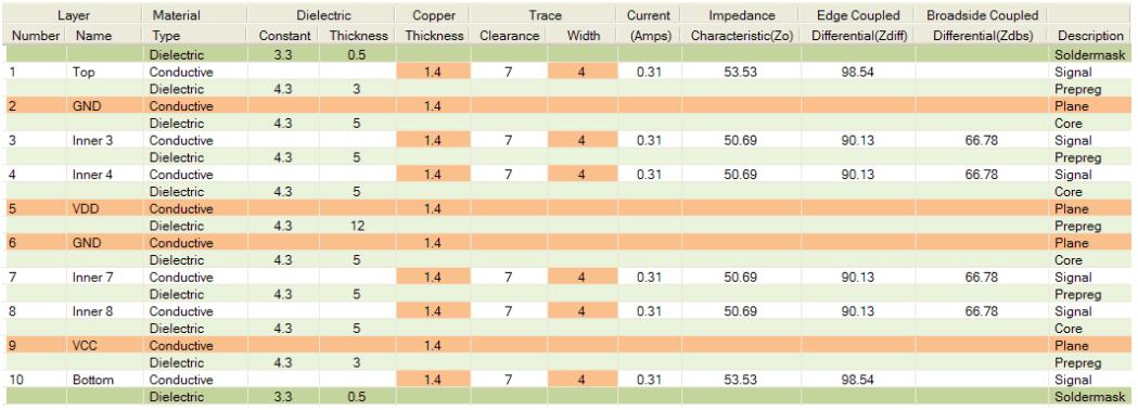
A typical 10 layer overlay is shown above. This superposition is ideal because of the tight coupling of the signal and returns plane, the shielding of the high-speed signal layer, the presence of multiple ground planes, and the symmetry of tightly coupled power/ground at the center of the circuit board. High-speed signals are usually routed on signal layers buried between planes (in this case, layers 3-4 and 7-8). However, care should be taken to route these signals correctly. Other, avoid coupling (crosstalk) between adjacent layers.
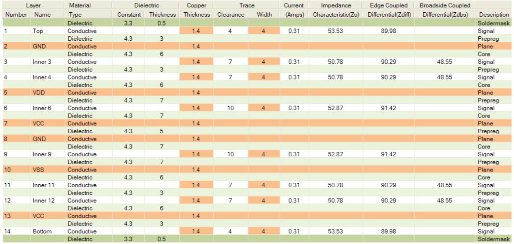
12 layer PCB stack
12 layers are the maximum number of layers that can be easily made in 62mil thick PCB. Occasionally you’ll see 14 to 16 layers of boards made into 62mil thick boards, but the number of manufacturers that make them is limited to those who can make HDI boards. The above twelve stacked layers provide shielding on six inner layers.
12 Layer PCB stack &14Layer PCB stack
When eight routing (signal) layers are required, a special critical shield is required to use the 14 layer overlay below. Layers 6 and 9 provide isolation for sensitive signals and 3, 4 and 11, 12 provide shielding for high-speed signals.
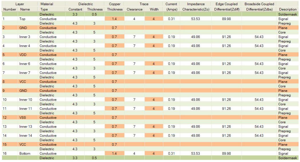
14 Layer PCB stack & 16 Layer PCB stack
16 Layer PCB provides ten layers of wiring, which are usually used in extremely dense designs. Typically, you will see a 16 layer PCB where the routing technology used in EDA applications cannot route the design to completion. "If it doesn’t route - just continue adding layers. ". Although this is a common saying, it is not a good practice.
If the board cannot complete the route, then there may be many reasons. Bad placement is often. Open the routing channels, reduce the number of crosses in the rat network, place vias on the 25 mil grid to allow routing and help routers as much as possible.
16 Layer PCB stack
The number of layers that can be manufactured is not actually limited to Multilayer PCB (please check the manufacturer’s function first). Of course, as the number of layers increases, the PCB thickness increases to accommodate the minimum thickness of the material used. The aspect ratio (board thickness and minimum hole size) must also be considered. Generally speaking, the thickness of 100 Mil material is 10:1. For example, a 200 mil thick substrate has a minimum hole size of 20 mils.
Determine the number of layers
The technical rule is based on the minimum spacing of SMT components used, which is basically the maximum routing, clearance and through-hole allowed while minimizing PCB manufacturing costs. Complex high-speed designs using a ball grid array (BGA) usually require 4 / 4 mil (routing/gap) and 20 / 8 mil (PAD/hole) via technology. However, if you can, use smaller sizes, which will reduce costs and increase manufacturing output.
Once these rules are established, the required characteristic impedance (Zo) and differential impedance required stack (Zdiff) are calculated according to the component datasheet. Typically, 50 ohm Zo and 100-ohm Zdiff are used. Keep in mind that lower impedances increase the di / dt and significantly increase the absorbed current (which is detrimental to the PDN), and higher impedances generate more EMI and make the design more susceptible to external influences. Therefore, a good Zo range is 50-60 ohm.
The total number of layers required for a given design depends on the complexity of the design. Factors include the number of signaling networks that must break through from BGA; the number of power supplies required by BGA; component density and package type.
Experienced designers will know about it after a while, but checking that there are enough layers is a good way to automatically adjust the board. If not adjusted, the router needs to complete at least 85% of the routing to indicate that the selected stack is routable. You may need to reevaluate the placement several times for the best results.
Learn More,
How to optimize PCB manufacturing cost when you design PCB
What are the advantages of manufacturing PCB in China
How to price and quote PCB?