


How to design an RF PCB? Some common sense you need to know as a novice
Radio frequency (RF) devices are one of the most exciting applications in electronic design right now. Any emerging technology for smartphones, sensors, robotics, and security will require these complex, high-frequency circuit boards. But as we all know, RF PCB design is a complex process that involves many considerations and design ground rules to ensure signal integrity, reduce interference, and maintain efficiency.
1.RF PCB design Basic rules for RF PCB design
When designing RF PCB, I think you need to know some basic rules:
A. All components should be surface mounted as much as possible 2.Sirf reference typical four- and six-layer boards, standard FR4 material
B. When placing connectors, try to avoid introducing noise into the RF circuit, try to use small connectors, and properly ground
C. All RF devices should be placed closely to keep the connection short and the crossover minimum (critical)
D. All pins should be strictly in accordance with reference schematic. All IC power pins should have 0.01uf decoupling capacitors, as close to the pins as possible, and must pass through holes to the ground and power layers
E. Reserve shielding space for RF circuits and baseband parts. The shielding should be connected continuously on the board and should be connected to the ground layer every 100mil (minimum)
F. The RF circuit should be separated from the digital part on the board
G. The RF ground should be directly connected to the ground layer, using dedicated vias and the shortest wires
H. TCXO crystal oscillators and crystal oscillator-related circuits should be strictly isolated from high slew-rate digital signals
I. Appropriate test points should be added to the development board
J. Isolate the RTC part from the digital and RF circuits, and the RTC circuit should be placed on the ground layer as much as possible
K. Use the same device for the version in the development process
L. PCB layout design needs to follow: ensure that the length matching, impedance control, space, width and differential pair routing are defined correctly. In this high-speed design, if the routing is not correct, we will see many problems, including crosstalk, EMI and EMC. (1) Proper return paths for all high-speed signals
(2) Proper ground reference
(3) High-speed signals should be routed on the same layer
(4) Try to keep tracks as short as possible
(5) Minimize vias
2. Things to consider before starting RF layout
When you start RF PCB layout, there are some typical considerations for any board. How big is the board? Where do key components or connectors need to go? How will it fit mechanically into the enclosure? These are important questions for any PCB, but RF systems have some unique design considerations that need to be answered.
3. High-frequency board design guide
A. Material selection: Common materials: Rogers series (such as RO4003C, RO4350B), Taconic, Isola, etc. High-frequency board materials have the following main performance characteristics:
(1) Low dielectric constant: The dielectric constant of high-frequency board materials is usually between 2.0-3.5, which is much lower than the dielectric constant of FR-4 materials (about 4.0-4.5), which helps to increase signal transmission speed and reduce signal loss.
(2) Low loss factor: The loss factor of high-frequency board materials is usually between 0.001-0.003, which is much lower than the loss factor of FR-4 materials (about 0.02-0.04), which helps to reduce energy loss during signal transmission.
(3) High heat resistance: The heat resistance of high-frequency board materials is usually above 200℃, which is much higher than the heat resistance of FR-4 materials (about 130℃), which helps to improve the reliability and stability of the circuit board. Select high thermal conductivity materials to achieve effective heat dissipation.
(4) Select materials with similar CTE to prevent warping and improve reliability.
It should be noted that high-frequency board materials usually have higher production costs. The main reasons are as follows: Raw material cost: The raw material price of FR-4 material is low, which helps to reduce production costs. Production process cost: The production process of FR-4 material is relatively mature and has high production efficiency, which helps to reduce production costs. Processing difficulty: The processing difficulty of FR-4 material is relatively small, and conventional processing methods can be used to reduce processing costs. Therefore, cost factors should also be considered when selecting high-frequency boards.
4. Stacking structure design
High-frequency circuits usually use multi-layer board structures to achieve good signal shielding and return paths:
When designing RF PCB stacking, the number of layers is an important consideration. Low-layer boards are generally not suitable for RF PCBs because they lack sufficient space to accommodate power, ground, and signal layers while meeting the target impedance requirements. Therefore, boards with higher layer counts are required.
For 2-layer boards, the limited space makes it impractical to accommodate printed circuits and impedance-controlled traces unless all wiring uses coplanar lines. This limitation poses a challenge to RF signal layout and routing, so 2-layer boards are not suitable for RF PCB design.
On the other hand, 4-layer boards are slightly better. In this configuration, all RF signals and components can be placed and routed on a single layer, while the bottom layer can be used for power, digital signals, and other peripherals. Alternatively, the bottom layer can be used for printed RF circuits at lower frequencies. If two signal layers are required, two inner layers can be designated for ground (GND) placement to provide isolation and impedance control on both layers.
For optimal RF PCB performance, six or more layers are generally recommended. This stackup allows controlled impedance routing on the outer surface layers, while plane layers provide shielding between signal layers. In addition, placing the power and ground planes adjacent to each other on the same side of the core enhances decoupling due to increased inter-plane capacitance. To ensure a consistent reference potential across the board, ground planes should be interconnected using stitching vias. In addition to considering the impedance of the RF signal line, the stacked structure of the RF PCB single board also needs to consider issues such as heat dissipation, current, devices, EMC, structure and skin effect. Usually, we follow the following basic principles in the layering and stacking of multi-layer printed circuit boards:
A) Each layer of the RF PCB is paved with a large area, there is no power plane, and the upper and lower adjacent layers of the RF wiring layer should be ground planes.
Even for mixed analog and digital boards, the digital part can have a power plane, but the RF area must still meet the requirement of large-area paving on each layer.
B) For RF double-sided boards, the top layer is the signal layer and the bottom layer is the ground plane.
For a four-layer RF single board, the top layer is the signal layer, the second and fourth layers are ground planes, and the third layer is for power and control lines. In special cases, some RF signal lines can be routed on the third layer. For RF single boards with more layers, the same can be applied.
C) For the RF backplane, the upper and lower surface layers are both ground. In order to reduce the impedance discontinuity caused by vias and connectors, the second, third, fourth and fifth layers are for digital signals.
The other stripline layers near the bottom are all bottom signal layers. Similarly, the two adjacent layers above and below the RF signal layer should be the ground, and each layer should be paved with a large area.
D) For high-power, high-current RF boards, the RF main link should be placed on the top layer and connected with a wider microstrip line.
This is conducive to heat dissipation and reducing energy loss, and reducing wire corrosion errors.
E) The power plane of the digital part should be close to the ground plane and arranged below the ground plane.
In this way, the capacitor between the two metal plates can be used as a smoothing capacitor for the power supply, and the ground plane also shields the radiation current distributed on the power plane.
5. RF board wiring requirements.
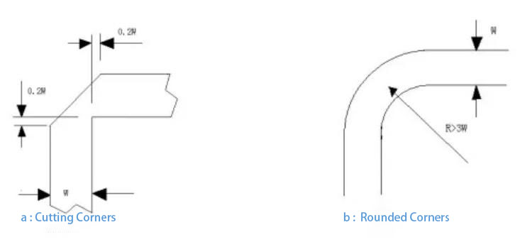
01 Shortest straight line principle:
If the RF signal routing is at right angles, the effective line width at the corner will increase, and the impedance discontinuity will cause reflection. Therefore, the corners must be processed, mainly by cutting and rounding.
(1) Corner cutting is suitable for relatively small corners, and the applicable frequency of corner cutting can reach 10GHz.
02 Microstrip line routing
The RF signal is routed on the top layer of the PCB. The plane layer below the RF signal must be a complete ground plane to form a microstrip line structure. To ensure the structural integrity of the microstrip line, the following requirements are met:
(1) The edges of the microstrip line on both sides must be at least 3W away from the edge of the ground plane below. And within the 3W range, there must be no non-grounded vias.
(2) The distance from the microstrip line to the shielding wall should be kept above 2W. (Note: W is the line width).
(3) The non-coupled microstrip lines in the same layer must be treated with ground copper foil and ground vias must be added to the ground copper foil. Find components in stock on Weiyang Mall. The hole spacing is less than λ/20 and is evenly arranged.
The edge of the ground copper foil should be smooth and flat, and sharp burrs are prohibited. It is recommended that the edge of the ground copper foil be greater than or equal to 1.5W or 3H away from the edge of the microstrip line. H represents the thickness of the microstrip substrate medium.
(4) The RF signal routing is prohibited from crossing the ground plane gap of the second layer.
03 Stripline Routing
RF signals sometimes need to pass through the middle layer of the PCB, most commonly through the third layer. The second and fourth layers must be complete ground planes, that is, eccentric stripline structures. To ensure the structural integrity of the stripline, the following requirements must be met:
(1) The edges of the stripline on both sides must be at least 3W away from the edges of the upper and lower ground planes, and there must be no non-grounded vias within the 3W range.
(2) RF striplines are prohibited from crossing the ground plane gaps of the upper and lower layers.
(3) Striplines in the same layer must be covered with ground copper foil and ground vias must be added to the ground copper foil. The hole spacing must be less than λ/20 and arranged evenly. The edge of the ground copper foil must be smooth and flat, and sharp burrs are prohibited.
It is recommended that the edge of the ground copper foil be greater than or equal to 1.5W or 3H away from the edge of the stripline, where H represents the total thickness of the upper and lower dielectric layers of the stripline.
If the stripline is to transmit high-power signals, in order to avoid the 50-ohm line width being too thin, the copper foil of the upper and lower reference planes of the stripline area is usually hollowed out. The hollowing width is more than 5 times the total dielectric thickness of the stripline. If the line width still does not meet the requirements, the upper and lower adjacent second reference planes are hollowed out.
6. Power and ground design
Integrity of ground layer: Ensure that the ground layer is not broken or divided to avoid interruption of return path.
Power partition and filtering:
Different circuit modules use separate power partitions.
Use decoupling capacitors and bypass capacitors to filter high-frequency noise.
Width of power and ground wires: Design power and ground wires that are wide enough according to the current size to reduce impedance.
7. Electromagnetic compatibility (EMC) design
Shielding and isolation:
High-speed signals should be as close to the ground layer as possible to form a shield.
Leave an isolation area between different functional modules to avoid interference.
Closed loop principle: Avoid forming a large area closed loop to reduce magnetic field radiation.
Filtering and protection:
Add common mode inductors or EMI filters at key interfaces.
Appropriately place TVS (diode) protection devices to prevent electrostatic discharge (ESD) damage.
8. Reduce vias: High-frequency signals minimize inter-layer switching to avoid introducing parasitic effects.
Via optimization:
Adjust the diameter and plating thickness of the vias to ensure mechanical strength and electrical performance.
Use ground via arrays to reduce ground potential differences.
9. High-frequency device layout
Priority: High-frequency devices should be arranged first and close to the signal input and output interfaces.
Compact layout: High-frequency devices and their associated devices should be as close as possible to shorten the length of the connection line.
Partition design: Analog circuits, digital circuits, and high-power circuits should be arranged in partitions to reduce mutual interference.
Through the above steps, a high-frequency circuit board with excellent performance and strong signal integrity can be effectively designed.


