


What is LDI?
LDI is a Laser Direct Imaging technology, which is mainly used in the exposure process of PCB process. It is different from the traditional negative contact exposure method. The most remarkable feature is that the negative is not used in the exposure process, and the graphics are transferred to the copper-clad laminate coated with " Photoimaging agent " by using the method of high-energy laser beam direct scanning.

Difference between LDI and traditional exposure
1. Traditional exposure is to transfer the image to PCB by irradiating the negative with a mercury lamp
2. LDI uses the laser scanning method to directly image the image on PCB, and the image is finer

Technical advantages of LDI
(1) LDI technology adopts laser positioning and vertical laser beam scanning, which can ensure that the graphic position deviation is within ± 5um, which greatly improves the line alignment accuracy and position.
(2) LDI technology does not use negative film, which can meet the production of very high-density fine conductors, improve the qualification rate of fine line PCB manufacturing and avoid repeated positioning defects.
(3) LDI technology does not need to manufacture, preserve and maintain photographic film devices, consumed materials, energy, other auxiliary materials, and chemicals, which reduces the production and processing cost.
(4) LDI technology can shorten the PCB manufacturing process, reduce the turnaround time, improve the rapid response-ability, reduce the intervention of human factors, simplify the operation process, and then improve the production efficiency.

Technical replacement of LDI
There is no doubt that the early adopters of laser direct imaging (LDI) technology are usually fast cycle, prototype, or high-capacity PCB manufacturers who need rapid and accurate prototype preparation.
These early direct imaging (LDI) models perfectly meet the needs of these PCB manufacturers - saving time and mask film cost while providing a high degree of flexibility and accuracy.
Mass PCB production manufacturers did not adopt LDI technology, mainly because the LDI system was too slow and the operation cost of adjusting mobile was too high. However, the latest technological development has changed the situation. Today, more and more mass PCB production manufacturers use LDI for imaging solutions.
LDI is used for imaging requirements for HDI PCB mass production
In order to meet the requirements of HDI PCB mass production, the imaging method shall:
1. While achieving a low defect rate and high output, it can achieve the stable production of HDI PCB conventional high-precision operation. For example:
*Advanced mobile phone board, CSP pitch less than 0.5mm (with or without wires between BGA pads)
*The plate structure is 3 + N + 3, and there are stacked via hole.
In terms of imaging, such designs require a ring width of less than 75μm. In some cases, the ring width is even less than 50μm. Due to the alignment problem, these inevitably lead to low output. In addition, driven by miniaturization, the lines and spacing are becoming thinner and thinner - meeting this challenge requires changing the traditional imaging methods.
This can be done by reducing the panel size or use a shutter exposure machine for panel imaging in several steps (four or six). Both methods achieve better alignment by reducing the influence of material deformation. Changing the panel size leads to high material costs, and using the shutter exposure machine leads to low production every day. Neither method can completely solve the material deformation and reduce the defects related to the photographic film, including the actual deformation of the photographic film when printing batch boards.
2. As mentioned earlier, the relevant quantity of the required yield should be taken into account in the accuracy requirements. To achieve the required output, high yield rates need to be achieved through automatic control.
3. Low-cost operation. This is the main requirement for any batch PCB manufacturer. In the early LDI mode, either the traditional dry film is required to be replaced with a more sensitive dry film to achieve faster imaging speed, or the dry film is replaced with a different wavelength band according to the light source used in the LDI mode. In all these cases, the new dry film is usually more expensive than the traditional dry film used by the PCB manufacturer.
4. Compatible with existing processes and production methods. Batch production processes and methods are usually carefully specified to meet the requirements of batch production. The introduction of any new imaging method should minimize the change of existing methods. This includes the traceability function of minimizing the change of dry film used, the ability to expose each layer of solder resist film, and batch production requirements.
The latest LDI technology
The latest LDI development overcomes the limitations of early LDI technology and provides practical solutions to the requirements of mass production.
1. Accuracy
LDI has proved to be much more accurate than using the existing shutter exposure machine. Like the new design and stacking technology enter mass production from the R & D stage, it requires higher precision imaging methods. Figure 1 shows the changes from very complex design to mass production. When using the shutter exposure machine, it takes multiple steps to expose a panel. In these cases, the advantage of LDI is that it can complete the precise alignment imaging on a large panel in one step without wasting time in multiple steps. The following photos of metallographic sections compare the results obtained by the shutter exposure machine (Fig. 1) with the accurate results obtained by LDI (Fig. 2).

2. Output
The latest technological development of electronic products, along with the improvement of laser power supply (from 4W to 8W), can now enable LDI to meet the high-yield requirements of HDI PCB production. The doubling of laser power supply enables PCB manufacturers to obtain high imaging output while continuing to use their traditional dry film.
Table 1 shows the daily output (produced in 22 hours) obtained by the LDI of a household 8W laser and the output obtained by the LDI of the same PCB manufacturer using a 4W laser. The energy settings are different (15 MJ / cm2, 30 MJ / cm2, 45 MJ / cm2, and 60 MJ / cm2), and the minimum body size is 50μm.
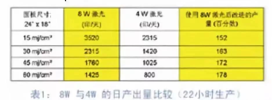
The output can be improved by 50% to 80% using an 8W laser, and the traditional dry ink is used, which has a ring width of less than 75μM advanced HDI with precision alignment requirements is a great improvement. When using 15 MJ / cm2 LDI dry film and 8W laser for the LDI machine, the output can reach 3500 prints/day and meet the high accuracy requirements of precision alignment. It is surprising to see these. Table 2 shows the daily output and 4 steps of 8W laser (used to achieve the required accuracy in advanced HDI PCB design) Comparison of the daily output of shutter exposure machine. The table shows that in some cases when the accuracy requirements are very high, the daily output of one set of 8W laser LDI machines can exceed that of one set of two shutter exposure machines!
The output of the shutter exposure machine in Table 2 is calculated as [4 * (positioning time + exposure time) + operation time]. Positioning time = 10 seconds, exposure time = 3 seconds, operation time = 6 seconds.

3. Auto-Control
Obviously, automatic control is the basic requirement of any imaging method for mass production and the necessary condition to achieve high output. The requirements of automatic control are different for each customer in all aspects.
Automation concept - stand-alone or inline, with a flipper or without;
Automatic control equipment suppliers - different PCB manufacturers want to cooperate with their own automatic control equipment suppliers, and other specific requirements of customers - machine size limitations, panel size, panel thickness, and more.

In order to meet all different requirements, automatic control interface solutions for LDI have been developed. Users around the world have adopted different automatic control measures for LDI machines. There are two main use modes: independent automatic control equipment - automatic control equipment connected with one machine for picking up and placing.
Split automatic control - automatic control equipment connecting two machines for picking up and placing. One of the two machines has a turnover machine to form an exposure unit with one side entering the board, both machines for exposure and one side out of the board.


Orbotech LDI
4. Low-cost operation
The latest dual laser power supply (8W) technology can not only produce higher output but also use low-sensitive dry films. In fact, PCB manufacturers can use their existing low-cost dry films. There is no need to replace the dry films with faster and more expensive LDI dry films. We can continue to use the dry films used in the current process and maintain the same output at the same time.
In some cases, the output can even be improved compared to other imaging methods such as shutter exposure machines. Which is a big breakthrough for the LDI system used in HDI PCB mass production.
5. Compatible with existing processes
PCB manufacturers often find it difficult and troublesome to introduce LDI technology into mass production. The latest LDI technology solves some common problems for manufacturers considering introducing LDI into production:
Q: Do I have to change the dry film I use now?
A: The development of 8W laser technology in a 355 nm industrial standard band enables suppliers to continue to use existing dry films while meeting the required daily output.
Q: The dynamic scaling function of LDI is good for the outer layer graphics, but will it cause more problems for the exposure of solder resist film?
A: In order to solve this requirement, several measures are used.
Solder resist exposed with LDI - this is the final solution to this problem. Major solder resists manufacturers, such as Taiyo, Tamura, Huntsman, and Sun Chemical, have developed fast LDI solder resist with sensitivity ranging from 40 to 70 MJ / cm2, especially in HDI applications.
Q: Different scaling modes
A: When the newly developed LDI solder resists is not applicable or needs time to verify the new solder resist, the developed advanced LDI scaling mode enables the operator of the LDI machine to limit the dynamic scaling to segmented scaling groups, resulting in only a few groups of panels in each batch. In the later stage of the process, it is easy to generate photographic plates (films)To expose each group, because it is known that the scale factor of each group is generated by LDI and has been printed on the panel during the exposure of outer graphics.
Q: Traceability tools are necessary for mass production. Can LDI support this requirement“
A: The latest technology of LDI includes special tools to support mass production. LDI's digital printing has special functions, which are impossible to obtain using photographic plates. The imaging method of each panel makes it unnecessary to cover all panels in a batch with a "negative", which gives LDI special personalization features, printing dynamic series numbers, date markers, scale marks.
LDI for production summary
With the increasingly strict and precise alignment requirements, it is necessary to replace the traditional exposure methods. The latest developments in LDI technology, such as all requirements on mass production, can be achieved through LDI, including accuracy, output, automatic control, and traceability.
Although mass production of HDI boards requires high acquisition costs to purchase LDI equipment, the growing team of HDI manufacturers is now using the LDI system as the imaging method of the mass production line. The reason is simple: these manufacturers have confirmed that LDI has increased their production by at least 3% on some more complex HDI boards, and the result is that they can recover their investment within a year.


