


A Brief Primer on HDI PCB Manufacturing
HDI is the abbreviation for high-density interconnectors. It refers to technology for manufacturing printed circuit boards (PCB). Based on traditional multi-layer printed circuit board manufacturing technology, HDI introduces a new process of foil-RCC (Resin Coated Copper) laminate, supplemented by laser drilling, horizontal/vertical PTH (Plated Through Hole) wet process, and other processes produced by the blind hole/multi-layer buried PCB circuit boards.
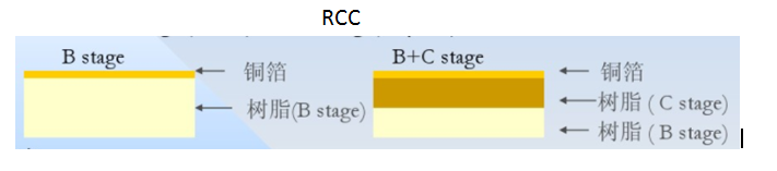
RCC (Resin Coated Copper) is a new product free from glass fiber, which facilitates and plasma etching treatment and makes multi-layer boards lightweight and thin. The copper foil of RCC is generally 18μm 12μm, or even 8.75μm, which is easy to process.
Holes less than 150um in diameter are known in the industry as microvia. Microvia geometry technology can improve the efficiency of circuits’ assembly and space utilization, and results in the miniaturization of electronic products.
PCB circuit boards manufactured with this type of structure have been referred to by several different names by the practitioners of the industry. European and American businesses have referred to such products as SBU (Sequential Build-up) boards because the programs they are producing are structured in a sequential manner. As for the Japanese side, because the hole size of the technology is much smaller than its previous generation, it is called MVP (micro via process). Some people called boards of this type BUM (Build-up Multilayer) boards to distinguish them from traditional multi-layer boards (MLB). The IPC Board Association of the United States, in order to avoid confusion, proposed that such products be called HDI boards as a generic name.
Characteristics of HDI PCB circuit boards
1. The trace distribution is excellent, and trace width/space can be 0.1mm or less;
2. The diameter of electroplating holes can be as little as 0.07-0.3mm;
3. The thickness of finished 6-layer PCB circuit boards can be less than 0.7mm.
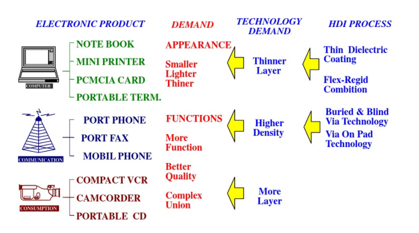
The development of HDI PCB circuit boards has been on a path towards delicacy, compactness, and thinness, providing technical precondition for high-quality transmission of communication signals. In view of the characteristics of HDI products, it is mainly used for mobile phone motherboards, computer components, and telecommunication equipment. HDI has been introduced as a high-end technology of PCB fabrication in recent years.
Advantages of HDI PCBs
Reduction of PCB fabrication costs
Although the number of layers of PCB circuit boards has reached more than eight, the cost of HDI PCBs manufacturing is lower than traditional complex lamination processes.
Increase in line density
The interconnection between traditional printed circuit boards and components must be achieved by the lines drawn around QFP (Quad Flat Package) and through-hole conductors (Fan-in and Fan-out), hence these lines will have to inevitably occupy some space.
However, micro via technology can embed the interconnection wiring in the following layer without Fan-in and Fan-out. Therefore, some pads (such as mini-BGA or CSP ball welding) can be placed on the surface of the outer panel to integrate more parts, which can increase the density of the printed circuit board. At present, this new stack and layout method has been used in many small but powerful telephones.
Favorability for the use of advanced construction technology
The conventional mechanical drilling technology cannot meet the needs of the new generation of small parts of fine lines because of the large size of the pad. With the progress of micro-hole technology, designers can use the latest high-density IC construction technology, such as Array package, CSP (Chip Scale Packaging), and DCA (Direct Chip Attach).
Better electrical performance and signal correctness
In addition to reducing the reflection of signals and cross-talk interference between lines, and increasing the space for circuit board design, the use of micro via interconnection can reduce the effect of inductance and capacitance, and the switching noise in signal transmission because the physical structure of the micro via is small and short.
Improvement in thermal properties
Glass transition temperature (Tg) refers to the temperature below which the physical properties of plastics change to those of a glassy or crystalline state. HDI dielectrics have higher glass transition temperatures, so they have better thermal properties.
Improvements in RFVEMV/ESD
Microvia technology can shorten the distance between the ground layer and the signal layer to reduce the interference of radiofrequency and electromagnetic waves. Moreover, it can increase the number of grounding wires and avoid damage of parts in the circuit caused by instantaneous discharge due to electrostatic accumulation.
Improvement in design efficiency
Microvia technology allows the lines to be arranged in the inner layer so that the design efficiency can benefit from more design space.
Typical HDI structures
Microvia technology, a part of HDI technology used in the sequential lamination, can result in ultra-thin multi-layer circuit boards with high density interconnect structures, which can now be divided into three categories.
1. Photosensitive hole technology (photo via)
2. Plasma etching
3. Laser ablation/drilling
As for laser drilling technology, it is one of the most spectacular technology developments in the global high-density connected circuit board industry. Generally, it can be divided into three categories.
1. CO2 Laser drilling
2. Nd: YAG Laser drilling
3. Excimer/ Excited dimmer
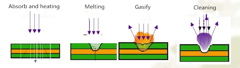
Introduction to CO2 Laser drilling technology
With certain power and discharge time, CO2 gas can generate pulsed infrared lasers with wavelengths ranging from 9,400 to 10,600nm. Infrared radiation is renowned for its ability to penetrate the surface to the interior of most organic materials. At the same time, most organic materials have a strong tendency to infrared absorption and energy generation, which is known to be the thermal effect of infrared. CO2 laser drilling rig is to make use of such effect to burn organic matter and form a connected blind hole.
Drilling Methods for CO2 Laser Hole Formation
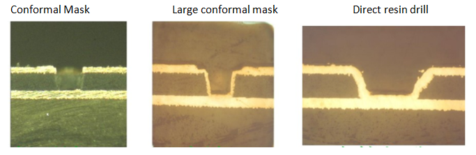
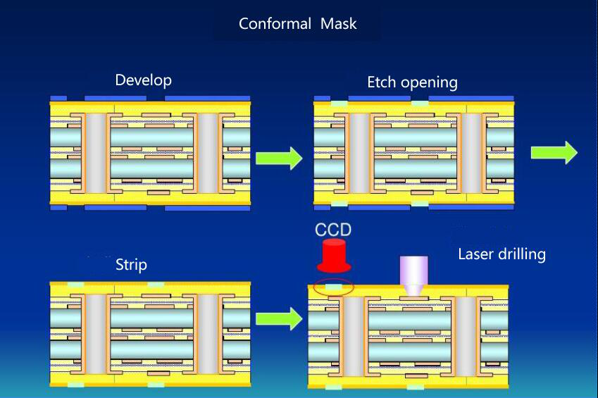
1. Open window method (Conformal Mask)
This method presses RCC on the inner core board first, opens the copper window, and then burns the substrate in the window with laser light to complete the micro-blind hole. Details are to make FR-4 inner core board with blackened surface and backing (Target Pad) on both sides, and then press an RCC on each side. The copper foil in this Resin Coated Copper Foil is 0.5oz, and the thickness of the adhesive layer is about 80-100um (3-4mil). Then, the resin in the window can be burned off by using CO2 laser light according to the coordinate program of the etched copper plate, and the bottom pad can be hollowed out to form a micro-blind hole.
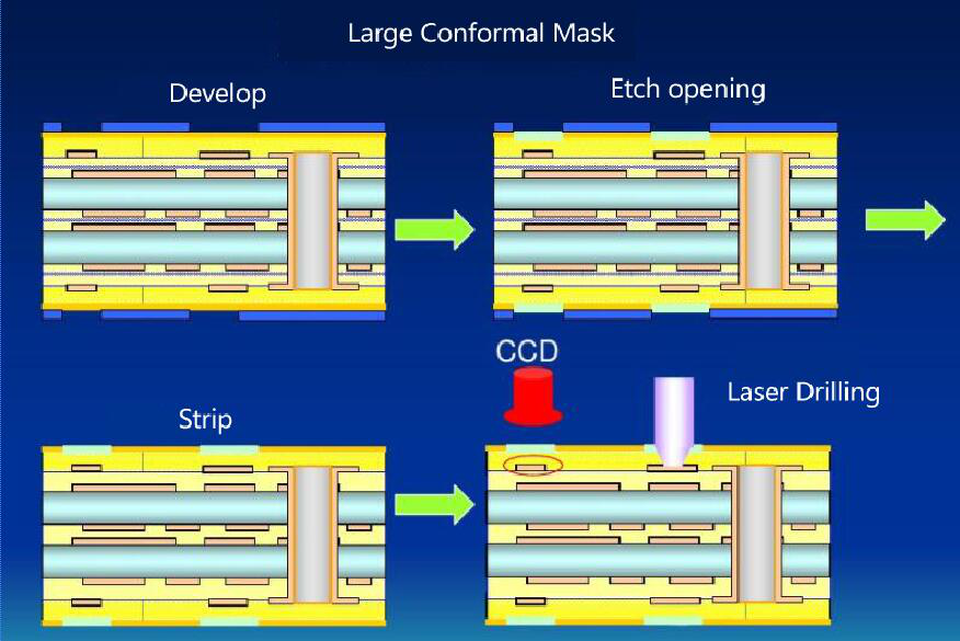
2. Large conformal mask
The aperture in the conformal mask method is the same as that of the copper window, so once the position of the window has deviated, it will lead the blind hole to move and cause misregistration of the base pad.
The deviation of these copper windows may come from the film problem of plate expansion and shrinkage and image transfer. It is not easy to solve the problem thoroughly on the large plate surface.
The so-called "large conformal mask" is to expand the hole size to about 2 mils more than the bottom pad. Generally, if the aperture is 6mil, the base pad should be about 10mil, and its window can be opened to 12 mils. Then, the coordinate data of the underlying pad of the inner layer are handed over to the laser for use, so that the position of the micro-blind hole of the underlying pad can be accurately aligned. That is to say, the large window has more space so that the hole position can obtain more elastic space. Laser light is then able to form holes according to the procedure of the underlying pad, without having to completely follow the window position to burn the hole that has been taken.
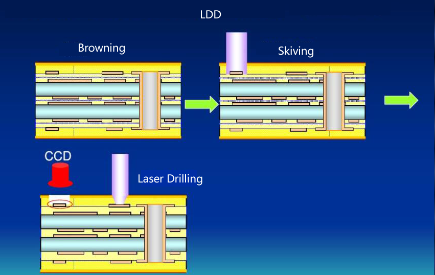
3. Copper direct burn-through method
After pressing the RCC copper foil on both sides of the inner core board, the original 0.50Z (17um) copper foil can be reduced to about 5um in thickness by Half Etching, and then the black oxide layer and direct hole formation can be made.
Due to the strong absorption of black surface, under the ultra-thin copper layer and the beam energy of the increased CO2 laser, the copper will be pierced directly into the substrate to form a hole, but it is not easy to achieve excellent "half-etching". To our content, the existing copper foil industry provides a special solution known as "paste copper ultra-thin copper foil" (such as the tearable UTC of Mitsui, Japan), the HDI semi-finished product with ultra-thin copper skin (UTC) can be obtained directly.
Introduction to Nd: YAG Laser Drilling
Nd: YAG is a kind of UV laser produced by Nd and Yttrium aluminum garnet crystals. Laser beams driven by diode pulses are commonly used nowadays, which can be used to make an effective laser sealing system without water cooling. The most distinctive characteristic of this type of laser drilling is that it adopts ultraviolet. The copper foil and glass fiber made of copper-clad laminate have strong absorbance when exposed to ultraviolet. In addition, featuring a small light spot and large energy, it can penetrate the copper foil and glass cloth strongly and make holes directly. Because the laser heat is small, it will not generate carbon slag after laser drilling, which provides a good surface treatment for the subsequent process of the hole wall.
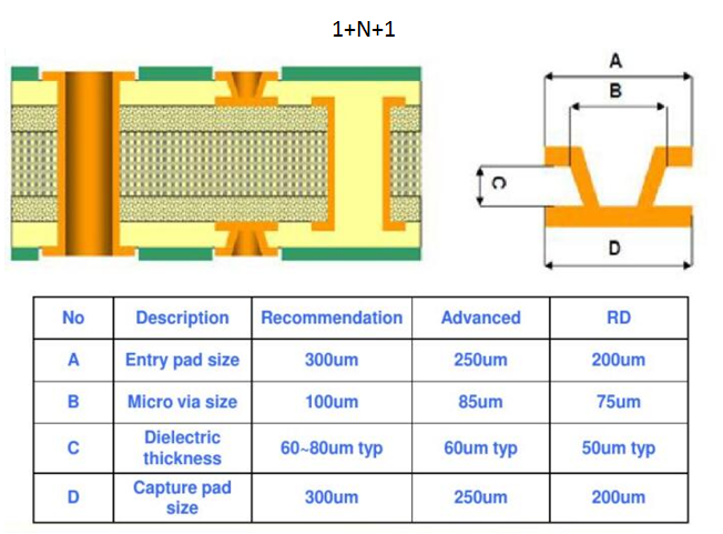
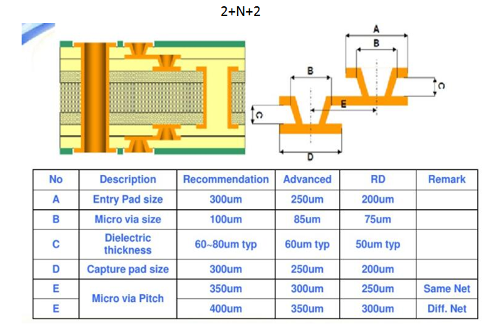
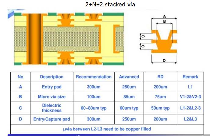
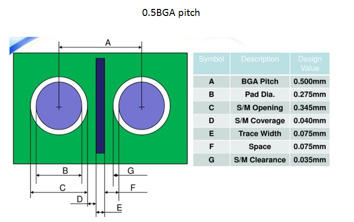
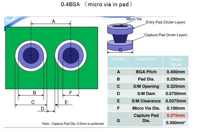
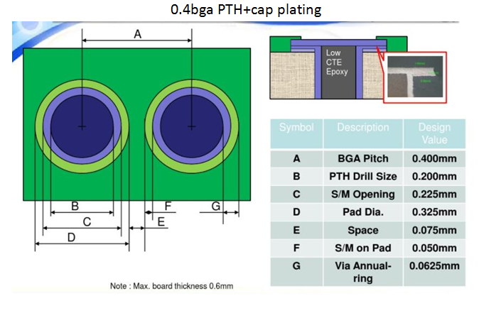
Recommended Design Dimensions of HDI Microvia
Features of Build-up Structures
· HDI microvia boards
-Typical applications: Engine boards, sub modules/boards
-6-10 Layers
· Availability of Various Technologies
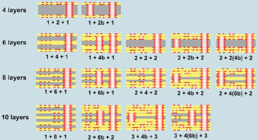
a. Staggered Sequential Build-up boards (1-nB+1, 2+nB+2…)
-Good availability, mature technology
-Limitations in routing capability
b. Stacked Sequential Build-up boards (2+nB+2, 3+nB+3)
-Reasonable availability, good routing capability, wide thickness variation
-Higher cost compared to staggered
c. Any Layer HDI
-E.g. ALIVH (Any Layer Inner Via Hole), B2it (Buried Bump interconnection technology), FVSS (Free Via Stacked Up Structure), etc.
-Excellent routing capability
-Limitations in availability cost/area
Development Trends of Build-up Structures
1. Increase in layers
2. More concise design and thinner PCB circuit boards
3. Increase in use of FPC boards and rigid-flex build-up
4. Higher level of integration
5. PCB applications must satisfy increasing requirements
6. Better performance and functionalities
7. Better temperature control and reliability
8. Faster replacement cycle
It is expected that the mainstream of HDI PCB fabrication will be developed towards high density and environmental friendliness featuring lead-free and halogen-free, which will benefit the following aspects:
1. Line width/spacing will change from 4mil/4mil which is the mainstream at present to 3mil/3mil and 2mil/2mil in the future.
2. Minimization of hole size, from 4mil to 3mil and 2mil
3. Multistage of HDI, from 1 stage to the forthcoming 2 or 3 stages
General Requirements for HDI PCB Material
1. Halogen-free materials
2. Process registration because of stricter tolerance requirements
3. Surface flatness
4. Laser drilling capability
5. Stricter electrical properties
6. Proper coefficient of thermal expansion (CTE)
An Overview of Global Market of HDI PCBs
At present, HDI accounts for 12.5% of the world's PCB circuit board output of 72.5 billion US dollars and has a market scale of about 10 billion US dollars (2018). It is mainly used in mobile electronic devices (such as mobile phones, tablets, smart wearable devices, etc.), computers and peripherals (such as high-end desktops, laptops, servers, memory, etc.), automotive electronics, and telecommunication equipment. The category of mobile electronic devices (especially mobile phones, according to IDC data), which shipped 1.97 billion global functions and smartphones in 2017, including 1.462 billion smartphones), is the largest application area of HDI, and also the most demanding area of HDI technology (such as Any Layer, SLP), will also lead the direction of HDI technology development in the future.
At present, more than 100 companies are estimated to produce HDI PCB in the world (80% of the top 100 PCB makers in the world introduce HDI), and the total output value in 2017 is about 9 billion US dollars. In terms of PCB fabrication, HDI products are mainly manufactured in China’s mainland (about 52%), Taiwan (about 23%), Korea (about 12%), Japan (about 6%). By region, HDI products are mainly manufactured in Taiwan (about 36%), Hong Kong and China’s mainland (about 14.5%), South Korea (about 16%), Japan (about 13%), the United States (about 10%), and Austria (about 8.5%).
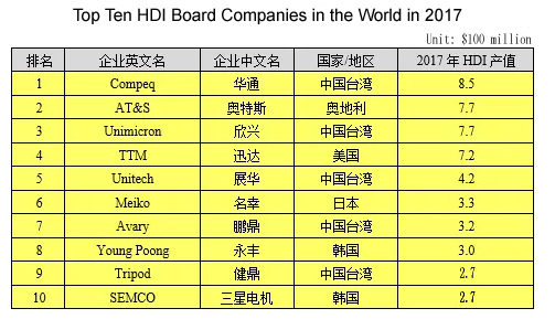
The world's top HDI manufacturers are basically diversified PCB products, that is, the non-single HDI manufacturing business, the world's top 10 HDI manufacturers accounted for about 56% of the world's total HDI output value. It belongs to the low concentration oligopoly type.
Currently, there are nearly 20 HDI companies in China’s mainland, including GOWORLD, Founder, Multek, Shengyi Electronics, Topcb, Bomin, Suntak, Kingwong, and Rocket PCB, etc. The overall scale of domestic HDI PCB fabrication has been steady growth in China from low-end HDI products to SLP, Any Layer, and rigid-flex HDI.


