


RF board laminated structure and RF board wiring requirements
RF Plate Laminated Structure
In addition to considering the impedance of RF signal lines, the laminated structure of RF PCB also requires to consider heat dissipation, current, device, EMC, structure, and skin effect. Usually, we comply with the following basic principles in the layering and stacking of multilayer printed boards.
Each layer of the RF PCB is paved with a large area, with no power plane. Both upper and lower adjacent layers of the RF wiring layer should be the ground plane.
Even the digital part can have a power supply plane, but the RF area still has to meet the requirements of a large area of ground connection on each layer.
For the RF double layer board, the top layer is the signal layer and the bottom layer is the ground plane. Four-layer RF board, top layer for signal layer, second and fourth layers for the ground plane, third layer walking power supply, control line. In a special case, you can walk some RF signal lines on the third floor. More layers of RF board are the same.
For RF Backplane, both the upper and lower surface layers are ground, in order to reduce the impedance discontinuity caused by the vias and connector. The second, third, fourth, fifth layer walks the digital signal. And all the other ground-bottomed ribbon layers are RF signal layers. Similarly, Two layers adjacent to the RF signal layer are the ground, each layer should be a large area of ground.
For a high-power, high-current RF board, the RF main link should be placed to the top layer and connected with a wide microstrip line, this is beneficial to heat dissipation and reduce energy loss, and reduce wire corrosion error.
The power supply plane of the digital part should be close to the grounding plane and arranged under the grounding plane, this allows the capacitance between the two metal plates to be used as a smoothing capacitor for the power supply, while the grounding plane also acts as shielding of the radiated current distributed on the power supply plane.
RF Board Cabling requirements
1. Corner
If the RF signal line goes to the right angle, the effective linewidth at the corner will increase, and the impedance is discontinuous and causes reflection, therefore, the corner should be treated, mainly for cutting angle and rounding corner two methods
The cutting angle is suitable for relatively small corners. As shown on the left, the tangent angle can be applied to a frequency of up to 10GHz.
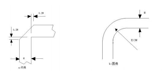
The radius of the arc angle should be large enough, in general, to ensure that: R>3W. As shown on the right
2. Microstrip Wire Wiring
The top layer of the PCB takes the RF signal, and the planar layer below the RF signal must be a complete grounding plane, forming a microstrip line structure. To ensure the structural integrity of microstrip lines, the following requirements are required,
(1) The edges on both sides of the Microstrip line must be at least 3W wide from the bottom ground plane edge. And in the 3W range, there must be no non-grounded vias
(2) The distance from the Microstrip line to the shielding wall should be maintained at more than 2W (Note: W for line width)
(3) The non-coupled microstrip line in the same layer should be treated with copper peel and add the vias on the copper peel of the ground. Hole spacing less than λ/20, evenly arranged.
Copper foil edges should be smooth, flat and no sharp burrs allowed
It is recommended that the edge of the copper peel is away from the edge of the microstrip line greater than or equal to the width of 1.5W or the width of 3H. H indicates the thickness of the microstrip substrate medium
(4) Banning RF signal wiring across the ground plane gap of the second layer
3. Ribbon wire Wiring
RF signals are sometimes passed through the middle layer of the PCB, and it is common to go from the third layer, and the second and fourth layers must be complete grounding planes. That is, the eccentric ribbon line structure, the structural integrity of the Ribbon line should be guaranteed to require
(1) The edges on both sides of the ribbon line are at least 3 W wide from the upper and lower plane edges, and in the 3W range, there must be no non-grounded vias.
(2) Banning RF ribbon lines crosse the ground plane gap of the upper and lower layers
(3) The Ribbon line in the same layer should be treated with copper peel and added vias to the ground copper peel.
Hole spacing less than λ/20, evenly arranged, the edge of the copper foil should be smooth and forbidden with sharp burrs. It is suggested that the edge of the copper peel is away from the ribbon line greater than or equal to the width of 1.5W or the width of 3H, H represents the total thickness of the upper and lower media layers of the ribbon line.
(4) If the ribbon line is to transmit high-power signals, in order to avoid 50-ohm line width, It is usually necessary to hollow out the copper skins of the upper and lower two reference planes in the Ribbon line area, the hollowed width should be 5 times more than the total media thickness of the stripline, if the line width still does not meet the requirements, the second layer of reference surface adjacent to the upper and lower sides is then hollowed out.


