


What is microvia?
Most PCBs are multilayer boards, and through holes are used to establish connections between each layer of the board. As the name suggests, microvia is the smallest through-hole with a size equal to or less than 150 microns drilled on PCB board by laser. In 2013, the IPC standard changed the definition of micro via to one with an aspect ratio of 1:1. The ratio of hole diameter to depth (not exceeding 0.25 mm). Previously, microvias were anything less than or equal to 0. 15 mm in diameter, so they usually span only a single layer.
Because the diameter is very small compared with the mechanical drilling through holes (PTH), we define them as microvias, which usually connect only one layer of the board to its adjacent layers.
These vias reduce the possibility of any type of manufacturing defect because they are laser drilled, thereby reducing the chance of any residue remaining after the process. Because of their small size and the ability to connect one layer to the next, they can make densely printed circuit boards that have more complex designs.
Microvia vs Via
Generally, vias with a diameter of less than or equal to 6mils are called microvias, which need laser drilling equipment. The diameter of ordinary Via holes is generally 8-20 mils, and mechanical drilling is used.
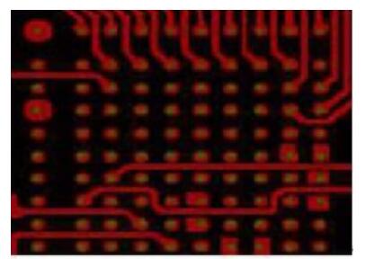
What are the types of microvias?
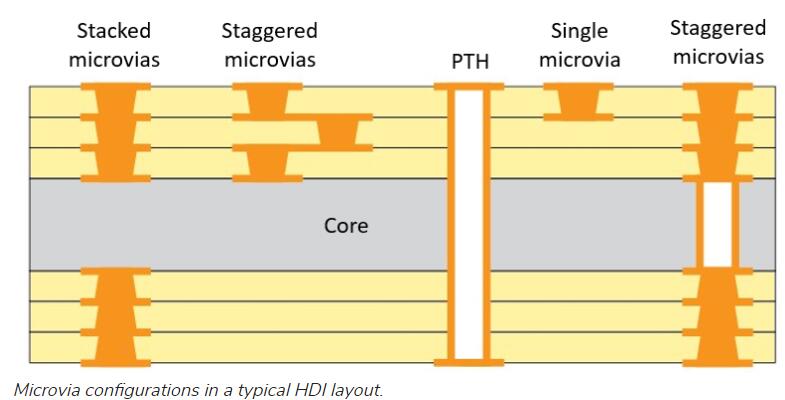
There are two types of microvias: stacked and staggered
These small structures enable the routing to reach the inner layer of PCB with higher interconnection density and a higher number of layers. These structures have existed for many years, but they are becoming more and more common in various systems where PCB needs to have multiple functions. If you have conducted a dimensional study and determined that about 6 million traces are required to install all components on a printed circuit board, it is inevitable that microvias will be used to route between the layers. This is how these structures are formed, and what you need to know about PCB microvias.
These holes are usually drilled by laser, and the process has been improved continuously. Due to their high output, they are the first choice in PCB manufacturing. The new development of laser drilling technology can reduce the number of micro holes to 15µm. The laser involved can only drill through one layer at a time. However, manufacturers use stacked microvias in multiple layers by drilling holes in individual layers and then stacking and compacting each layer.
In the PCB manufacturing process, compared with ordinary through holes, laser drilling micro through-holes have a lower possibility of manufacturing defects. This is because laser drilling does not leave any material in the hole. Mechanical drilling of micro through-holes may produce defects due to vibration caused by bit wear, while mechanical drilling of micro through-holes is only useful when the diameter is about 8 mils. In electroplating and reflow soldering, microvias do have the same risk as ordinary vias.
Therefore, it is very important to discuss the filling of tents or microvias with the manufacturer.
In addition to these qualities, the only differences between microvias are their typical diameter and their position on the circuit board. In this case, the distance between the balls is very small, and the dog bones will not be fanned out. The microvias on the surface layer can also be placed in the pad filled with conductive epoxy resin and plated with copper (called "VIPPO" or “POFV”). The advantage of the VIPPO copper structure is that the pad can be welded now, so it is an ideal choice for BGA with a spacing of about 4 mils.
Microvia in pad
Considering the distribution of microvia on the PCB, the following are different types of microvias.
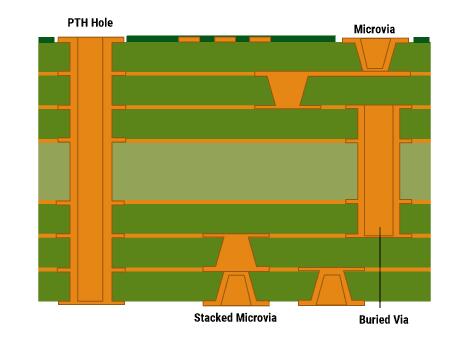
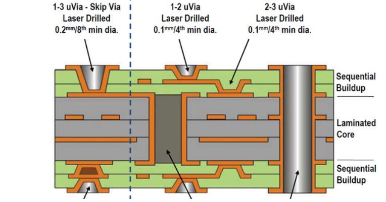
Blind microvias
The blind microvias start from the surface layer and end in one or two layers below the surface. It is best to place only one blind pore covering only a single layer. If you need to span 2 layers, it is better to use stacked microvias because they will be more reliable and require fewer manufacturing steps.
Buried microvias
The buried microvias span between the two inner layers and do not reach any of the circuit board surfaces. Just like blind holes, it is better to use buried microvias to span single layers to ensure reliability and ease of manufacture.
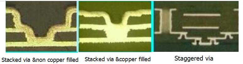
Stacked microvias
Stacked microvias are just stacked buried vias or blind microvias stacked on top of buried microvias. This is the standard method to span multiple layers in HDI PCB. The internal buried pores in the stack need to be filled with conductive adhesive and plated to ensure firm contact when depositing and plating the next via in the stack.
These types of micro vias have some special advantages in saving space and EMI.
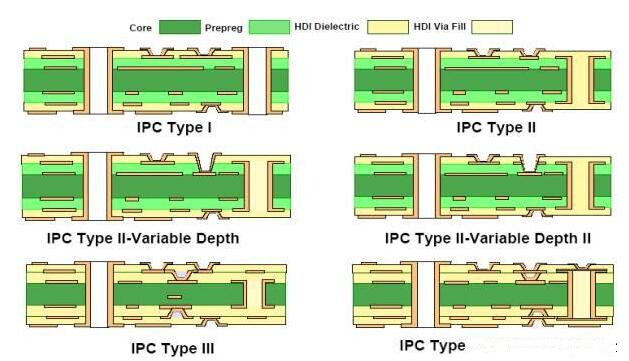
In IPC-2226, high-density interconnects are classified into six design types. They are grouped by stack characteristics in the following categories: type I, type II, type III, type IV, type V, and type VII
Type I, 1 [C] 0 or 1 [C] 1 with through holes from surface to surface.
Type II, 1 [C] 0 or 1 [C] 1, with via embedded in the core and possibly via connecting the outer layer from the outer surface to another surface.
Type III, 2 [C] 0, two or more HDI layers are added to the through-holes of the core or from one surface to another.
Type IV, 1 [P] 0, where p is a passive substrate without electrical connection.
V-type coreless construction using layer pairs.
Type VI uses layer pairs as an alternative to coreless construction
Rocket PCB's Mircrovia Advantages
In addition to the manufacturing difficulties of less advanced manufacturers, microvias are ubiquitous in HDI PCB, and they are responsible for saving space on these boards. For the thin spacing components in the dense board, they are required to ensure that the components can be installed in a small space. Circuit board space is money, and microvias can help you reduce costs. In addition to allowing tighter connections between layers and smaller routing, they also allow you to save space by placing vias directly in the pad. Microvias in pad can also save your space by connecting inside the pad of Surface Mount Technology (SMT). Because of its small size, micro through-hole is especially suitable for this. Sometimes, common vias are too large to accommodate SMT pads, such as BGA. The microvias can accommodate the inside of the pad without causing any manufacturing problems.
You may be hesitant to try to integrate a large number of burying and blind holes into your design, but microvias can change that. Traditional blind and buried holes will save you space but may be difficult to manufacture. However, because microvias have been fabricated layer by layer, they are ideal for embedded, blind, and stacked applications.
In addition to the BGA breakthrough, the micro via holes in the pad can even be inserted into the pad of the best spaced BGA, and they play an even greater role in the breakthrough channel. Even if you use the micro holes in the pad to save surface space, you still need many layers to keep these wires in other places on the board. The use of microvias can increase the width of the escape path and may allow you to use fewer layers to break through BGA.
We can't make better music, but we can reduce noise.
Rocket PCB support up to 40 laminates, laser drilling, micro via holes, stacked microvia holes, blind holes, buried through holes, via- in-pads, laser direct imaging, sequential lamination,. 00275 "trace / space, fine spacing as low as 3mil, controlled impedance, etc.
Able to produce HDI PCB without minimum order requirements and flexible turnaround time options. Each design is reviewed in detail by our cam engineers before production to ensure that there is no worry about the manufacturing process, and the support team is available 24 hours a week from Monday to Saturday to assist with your HDI PCB fabrication orders.
Advantages of EMI
Micro via has a great influence on the signal integrity of HDI circuit. The fact that the microvias have smaller parasitic capacitance and inductance due to their small size is a factor that makes them more tightly packed without increasing the crosstalk and noise coupling strength. When the HDI trace is close to the micropore, the smaller parasite will have a negative effect on the stronger electromagnetic field.
One of the major problems in high-speed circuits is the signal radiation and reflection in through holes. In addition, the resonance in the short through-hole tube will couple to the adjacent through-holes with high field strength. In essence, a larger via will form an antenna with larger radiation, especially when the signal is allowed to resonate in the stub. A good way to reduce antenna power is to reduce its size. Micro through-holes are basically like smaller antennas, so their emission and absorption cross-sections will be smaller than those of larger through holes. Microvias are made layer by layer, which means that there won't be any stubs (don't do that) unless you purposefully store them in them.
A great application of micro via is in the high-frequency transmission line. Take microwave and millimeter-wave stripline conductors as examples. They are suspended in the dielectric of the high-frequency circuit board and need through holes to elicit signals. Through holes introduce too much EMI to be used in higher frequency strip lines. In addition, compared with micro via, the via on microwave board will introduce significant insertion loss along with the interconnection, which is also due to the large capacitive and inductive coupling between the larger via and the reference plane nearby. High-frequency circuits are becoming more and more common. We will design more high-frequency circuits in the future. It's time to start mastering micro vias to control EMI on these types of boards.
Now that you have covered the microvias in printed circuit design, you need the right PCB design software to create your next HDI PCB. Altium Designer Can help you improve advanced PCB with microvias and a wide range of other tools.


