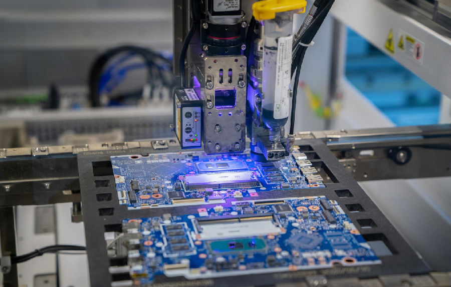
HDI processing capacity comes from Rocket PCB
HDI PCB manufacturing is the core manufacturing service of Rocket PCB. It has various functions, qualifications, certification, and professional knowledge, and can meet the most stringent requirements of HDI PCB manufacturing. Our extensive PCB manufacturing capabilities support the stringent requirements for advanced HDI PCB design in all industries, including medical, aerospace, defense, and commercial markets. (For more processing capabilities of PCB types, please refer to our PCB capability table)
Circuit Constructions | Single-Sided / Double-Sided / Multi-Layer / Flex / Rigid Flex |
Material | FR-4 / Rogers / Arlon / Polymide / Aluminum / Kapt/etc |
Copper weights | 0.5oz~10oz |
Layer Count | 1-64 layers |
Stack up | Control Dielectric/Control Impedance/TDR Testing/4+N+4/any layer |
Minimum Hole size | 4 mil |
Minimum trace space | 3mil/3mil |
Surface finish | Lead-Free/HASL/ENIG/ENEPIG/Hard Gold/Wire Bonded Gold/Immersion Silver/OSP/selective osp |
Vias | Blind-buried/via-in-pad/pofv/Filled-vias/epoxy resin filled vias |
Advanced tech | Embedded/Laser drill/Multi-level cavity/Bulid-up HDI/Long-short staged gold finger/Hybrid/metal core/press-fit |
Rocket PCB has advanced advantages in HDI PCB manufacturing. Advanced technology and equipment ensure that we can produce advanced HDI PCB. Would you like to know how much your HDI PCB manufacturing cost is? Please submit a quotation request on this page at any time and describe your HDI PCB requirements in detail. We will make a quotation for your HDI PCB soon.
Contact us for an HDI PCB quote
HDI types we support
We support up to 40 layers of lamination, laser drilling, microvias, stacked micro vias, blind vias, buried vias, vias in pads, laser direct imaging, sequential lamination, 00275 "trace/space, controlled impedance, etc. We are able to produce HDI PCB without minimum order requirements and flexible turnaround time options. Each design is carefully reviewed by our cam engineers before production to ensure that there are no worries about the manufacturing process. The support team provides you with HDI PCB manufacturing order assistance 24 hours a week from Monday to Saturday.
Rocket PCB has a scientific and perfect procurement chain. In order to ensure the quality from the source, we always insist on selecting high-quality PCB materials to produce all kinds of printed circuit boards. It has high safety and has passed the national compulsory certification. We provide customers with a worry-free purchase experience. Rocket PCB has a professional production workshop and exquisite production technology. Our HDI PCB meets the national quality Testing standard and high reliability. Various types include rigid board HDI 4 + N + 4 structure, any layer interconnection HDI technology, flexible board HDI and rigid-flex HDI board, which can fully meet the diversified needs of customers.
Advantages of HDI PCB
Reduce PCB manufacturing costs
Although the number of layers of PCB has reached more than eight, the manufacturing cost of HDI PCB is lower than that of the traditional complex lamination process.
Circuits density increase
The interconnection between traditional printed circuit boards and components must be around QFP (Quad Flat Package) and through-hole conductors (fan in and fan out) However, micro via technology can embed interconnect wiring into the next layer without a fan in and fan out. Therefore, some pads (such as mini BGA or CSP ball welding) can be placed on the surface of the outer panel By integrating more components, the density of the printed circuit board can be increased. At present, this new stack and layout method has been used in many small and powerful phones.
It is conducive to the use of advanced construction technology
The traditional mechanical drilling technology cannot meet the needs of the new generation of fine-grained small parts because the size of pads is too large. With the progress of microporous technology, designers can use the latest high-density IC construction technologies, such as Array Package, CSP (chip scale packaging) and DCA (direct chip attach).
Better electrical performance and signal correctness
In addition to reducing signal reflection and crosstalk interference between lines and increasing the space of circuit board design, the use of micro via interconnection can reduce the influence of inductance and capacitance and switching noise in signal transmission, because the structure of physical micro via is small and short.
Improve thermal performance
Glass transition temperature (TG) refers to the temperature at which the physical properties of plastics change to glassy or crystalline state. HDI dielectrics have higher glass transition temperatures, so they have better thermal properties.
Improvement of RFI / EMI / ESD
Microvia technology can shorten the distance between the grounding layer and the signal layer, reduce the interference of radio frequency and electromagnetic wave, and increase the number of grounding wires to avoid instantaneous discharge damage to parts in the circuit due to electrostatic accumulation.
Improve design efficiency
Microvia technology allows the lines to be arranged in the inner layer, so that the design efficiency benefits from more design space.
What is the application of HDI PCB?
HDI is widely used in mobile phones, digital cameras, MP3, MP4, household appliances, notebook computers, automotive motors, automotive control systems, automotive sensor applications, communication systems, network systems and other digital products, aerospace, among which mobile phones are the most widely used. One of the most critical areas for great progress in high-density PCB is the medical field. Medical equipment often needs high transmission Only HDI PCB can provide a small package of the transmission rate. For example, the implant needs to be small enough to fit the human body, but any electronic equipment involved in the implant must absolutely effectively allow high-speed signal transmission. In addition, other medical equipment, such as emergency room monitors, CT scans, etc., can also be used to HDI PCB.
Typical features of HDI PCB
1. The routing distribution is excellent, and the routing width/spacing can be less than 0.1mm;
2. The diameter of the electroplating hole can be as small as 0.07-0. 3mm;
3. The thickness of the finished 6-layer PCB can be less than 0.7mm.
4. Micro blind hole ring less than 6mil
5. The inner and outer wiring width shall be less than 4mil, and the pad diameter shall not be greater than 0. 35mm.
Types of microvias
1) PTH (electroplated through-hole): the hole connecting each layer of conductor.
2) Buried via: through-hole between local layers in multilayer board, called buried guide hole or buried hole.
3) Blind via (blind hole): part of the through holes in the multilayer board are deliberately not fully drilled because only a few layers are required to conduct, and some of them are connected to the hole ring of the outer board.
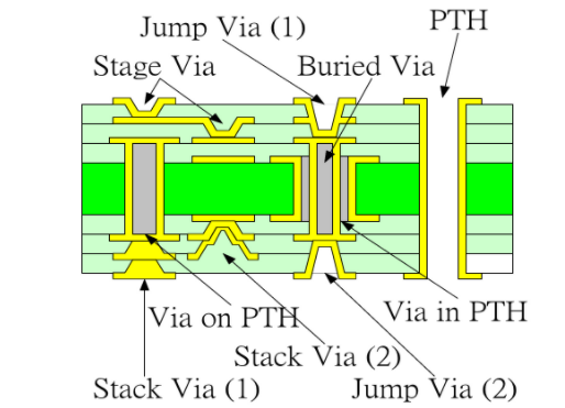
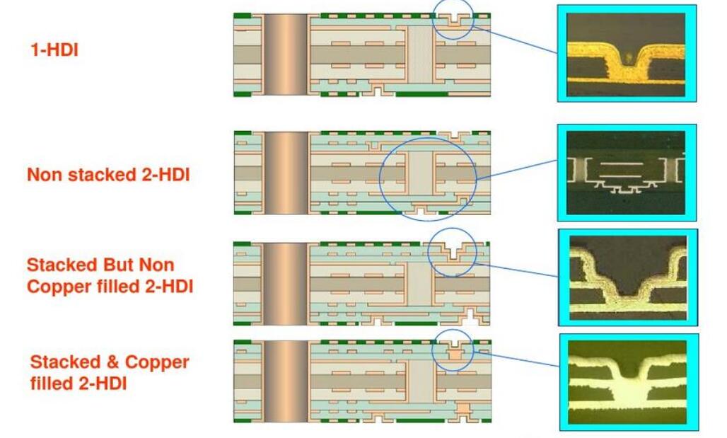
A. Stack via (stacked blind hole): the blind hole made in the first layer shall be plated with copper fill to connect with the blind hole in the second layer
B. Stage via (stepped blind hole): the second layer of the blind hole is punched on the receiving pad next to the first layer of the blind hole
C. Skipped via: the blind hole skips several layers and conducts a specific layer
D. Via on PTH: the blind hole is located on the buried hole, which needs to be plated flat to undertake radium perforation
E. Via in PTH: the hole in the hole. Fill the large hole first, and then make a small conducting hole in the middle. The plate made by the layer increasing method is named a + N + a. there is an interlayer of the core between them, which is added layer by layer outside. The plate can be added to two layers every time it is pressed.
How to define the stage of HDI
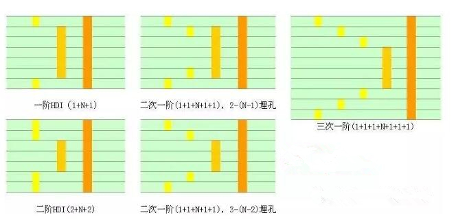
In the 6 laminates, the first and second stages are for the boards requiring laser drilling, i. e. HDI plates.
The first stage HDI board (1 + N + 1 HDI) refers to,
Blind holes: 1-2, 2-5, and 5-6, i. e. laser drilling is required for 1-2 and 5-6.
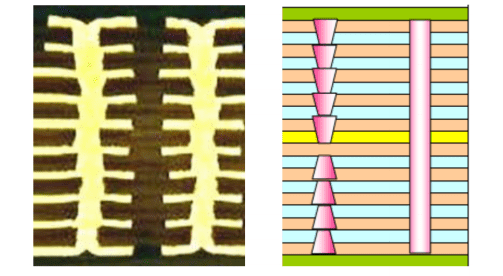
Two stage HDI PCB (2 + N + 2 HDI) refers to,
Blind holes: 1-2, 2-3, 3-4, 4-5, and 5-6. First drill 3-4 buried holes, then laminate 2-5, then drill 2-3 and 4-5 laser holes for the first time, drill 1-6 for the second time, and then drill 1-2 and 5-6 laser holes for the second time. Finally, drill through holes. It can be seen that the two sections of HDI PCB undergo two pressing and two laser drilling.
In addition, the two-order HDI board can also be divided into staggered two-order HDI boards and stacked two-order HDI boards. Staggered hole 2-order HDI board refers to the staggering blind holes 1-2 and 2-3, while stacked hole 2-order HDI board refers to the stacking of blind holes 1-2 and 2-3, such as blind holes: 1-3, 3-4 and 4-6. By analogy, 3-order and 4-order are the same.
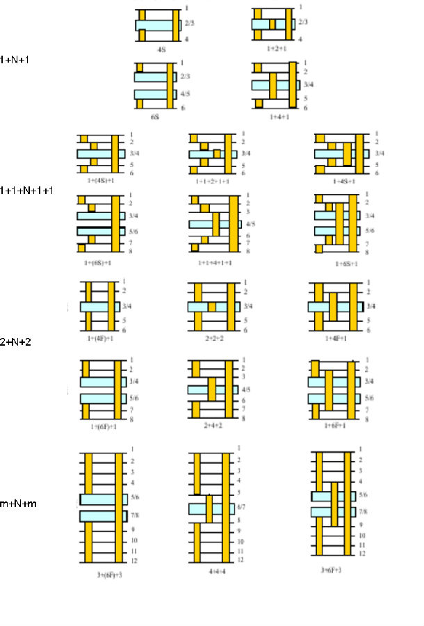
Typical HDI structure / Stack up
Anylayer(ELIC)HDI PCB
HDI PCB production process
Learn the detailed HDI manufacturing process from our pdf file, HDI PCB process.pdf.
Material of HDI PCB
HDI PCB puts forward some new requirements for PCB materials, including better dimensional stability, antistatic mobility, and non-viscosity. The typical material of HDI PCB is RCC (resin-coated copper). RCC includes polyimide metalized film, pure polyimide film, and cast polyimide film.
RCC (resin-coated copper) is a new product without glass fiber, which is convenient for plasma etching and makes the multilayer board light and thin. The copper foil of RCC is generally 18μm 12μm. Even 8. 75μm. Easy to process
There are two main types: B stage (Mitsui) and B + C stage (polyclad)
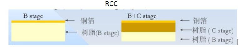
The advantages of RCC include small thickness, lightweight, flexibility and flammability, compatibility characteristic impedance, and excellent dimensional stability. In the process of HDI Multilayer PCB, it can replace the traditional adhesive chip and copper foil as an insulating medium and conductive layer. Traditional suppression technology can be used to suppress RCC. Then, non-mechanical drilling methods (such as a laser) can be used to form micro via interconnection.RCC promotes the emergence and development of PCB products from SMT (surface mount technology) to CSP (chip-level packaging), from mechanical drilling to laser drilling, and promotes the development and progress of PCB micro vias. All these make RCC a leading HDI PCB material.
In the actual PCB manufacturing process, FR-4 standard TG 140C, FR-4 high Tg 170C, and FR-4 and Rogers combined lamination is usually used most. With the development of HDI technology, HDI PCB materials must meet more requirements.
So, the main trends of HDI PCB materials should be:
Development and application of adhesive-free flexible materials;
The thickness of the dielectric layer is small and the deviation is small;
Development of LPIC;
The dielectric constant becomes smaller and smaller.
The dielectric loss is getting smaller and smaller.
High welding stability;
Strictly compatible with CTE (coefficient of thermal expansion);
Main manufacturing technologies of HDI
Special equipment and processes are required to produce HDI PCBs. These include laser drilling, plugging, laser direct imaging, sequential lamination cycles, and laser drills. HDI boards are thinner and have tighter lines. They also use smaller specialty materials. This type of board requires more time and significant investments in manufacturing equipment and processes to produce.
The difficulties of HDI PCB manufacturing lie in micropore manufacturing, through-hole metallization, and thin wire.
Micro via fabrication
Micro through-hole manufacturing has always been the core issue of HDI PCB manufacturing.
There are two main drilling methods:
1. For ordinary through-hole drilling, mechanical drilling has always been the best choice with its high efficiency and low cost.
2. There are two types of laser drilling: photothermal ablation and photochemical ablation. The former refers to the process of heating the working material after high-energy laser absorption, melting it, and evaporating through the formed through-hole. The latter refers to the result of high-energy photons in the ultraviolet region and laser length exceeding 400 nm.
Laser drilling technology
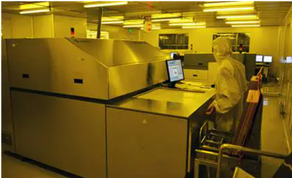
Unlike mechanical drilling, the laser drilling process does not physically contact the PCB material being used. Drilling the smallest pores can use more technology on the PCB surface. The high-impact beam of the UV laser can drill through copper and electromechanical media (PP, epoxy resin, adhesive, PI, EMI shielding film, etc.) To create tiny through holes. UV laser has excellent reflection, absorption, and transmission capabilities for different materials. The amount of laser drilling per square meter of HDI PCB has been very large. The density has even exceeded 50K/SQM and the drilling capacity of laser machine has always reached 4. 3 million pieces/day.
There are three types of laser systems for rigid-flex HDI PCB board: excimer laser, UV laser drilling, and CO2 laser. Laser technology is not only suitable for drilling, but also for cutting and forming. Although laser drilling equipment has a high cost, it has higher precision, stable technology, and mature technology. The advantages of laser technology make it the most commonly used method in blind / buried hole manufacturing. Today, 99% of HDI micro-holes are obtained by laser drilling.
PS laser drilling equipment
Through-hole metallization
The biggest difficulty of through-hole metallization is the difficulty of uniform coating. For micro through-hole deep hole electroplating technology, in addition to using the electroplating solution with strong dispersion ability, the electroplating solution on the electroplating device should be upgraded in time, which can be sprayed horizontally through strong mechanical stirring or vibration, ultrasonic stirring, and horizontal spraying. In addition, the humidity of the through-hole wall must be increased before electroplating.
In addition to the process improvement, the HDI through-hole metallization method also sees the main technical improvements: electroless plating additive technology, direct plating technology, etc.
VCP-Vertical continuous plating
Thin circuit
The realization of the thin lines includes traditional image transmission and laser direct imaging.
Laser direct imaging (LDI) technology
For LDI technology, there is no need for photographic film, and the image is directly formed on the photosensitive film by laser. UV wave lamp is used to avoid the adverse effects caused by film defects. CAD / CAM can be directly connected to shorten the manufacturing cycle, which is suitable for the production of a limited number of small-batch PCBs.
Imaging with finer or ultra-fine trajectories to process these HDI boards is expensive but necessary. Finer routing, spacing, and loops require stricter control. Modification, rework, or repair becomes an impossible task by using finer traces. Photographic tool quality, laminated prepreg, and imaging parameters are necessary for a successful process. LDI(laser direct imaging) is a better choice for this fine routing and spacing. The laser direct imaging (LDI) function ensures accurate registration, and all multi-layer cores are thoroughly inspected using automatic optical inspection (AOI) units for excellent defect detection of the finest features.
HDI PCB design guide
When designing HDI design, you should first refer to some available specification references, and IPC-related materials and specifications are one of the introductory materials for readers. IPC has four specifications that are highly relevant to HDI design:
1)IPC / JPCA-2315 - Guidelines for the design of high density interconnect structures and micro vias
2)IPC-2226-part of design criteria for high density interconnect (HDI) printed circuit boards
3)IPC / JPCA-4104 - Specification for verification and performance of dielectric materials for high density interconnect (HDI) structures
4)IPC-6016, specification for verification and performance of high density interconnect (HDI) structures
Readers who use HDI technology can refer to these specifications for technical planning and serve as an important reference for HDI design methods. IPC-2226 is a specification for educators on how to select pore-forming technology, circuit density, design criteria, interconnection structure and material characteristics. It attempts to provide some standards for the use of micro vias in circuit board design.
HDI board layout must take into account the minimum line width during production, the control of safety spacing (including line to line, line to pad, pad to pad, line to copper surface, etc.) and the uniformity of wiring, because the spacing is too small, in the inner dry film process (i. e. the process of transferring the inner pattern to PCB board) If the film cannot fade completely, it will cause short circuit of the line. The line width is too small and the adhesion of the film is insufficient, resulting in open circuit of the line. The uneven distribution of the lines on the same surface, that is, the uneven distribution of the copper surface, will cause inconsistent resin flow velocity at different points. The final result is that the copper thickness will be slightly thinner where the copper surface is less, and the copper thickness will be slightly thicker where the copper surface is more, so it should be noted in the design uniformity of wiring and copper laying.
The following are other related matters needing attention during wiring
1) The devices arranged in top layer and BOT layer have better isolation effect, so the mutual crosstalk between the inner layer change signals shall be avoided and reduced as far as possible;
2) For important signals such as RF and analog areas, ensure that there is a short return path of ground channel (up / down / left / right) around each signal, and more ground vias are drilled around such signals, so as to realize the nearest jump of return current and reduce the loop area.
3) Wiring area of important signals (such as clock / RF) (3w area with line width better) Blind holes without physical connection conflict shall not be added to avoid mutual interference, but blind holes of ground network can be added. This is because the insulation layer of HDI is thin, so it is difficult to press the plate. Where there are buried blind holes in the inner layer, the line is more likely to open circuit due to depression. Therefore, during design, the line shall try to avoid the position of buried blind holes, at least not from the middle of buried blind holes, if it is really unavoidable. Key signals and important signals must be avoided, such as clock signals, RF signals and high-speed signals, not only to ensure good process capacity, but also to avoid mutual interference between plates or other media although there are no physically connected holes and lines;
4) Due to the limited wiring space in the board, priority should be given to ensuring important signals and signals with impedance requirements The line width and line spacing of other signals can be appropriately reduced according to the actual space;
5) On the premise that the power supply meets the current capacity, the whole pavement shall be avoided as far as possible to reduce the interference to other signals;
6) If the production cost of PCB is given priority, the fan out of blind holes in the same network shall be kept at a distance of more than 3. 5mil from the pad, and the limit is 3mil; the distance between buried holes and blind holes, blind holes and through holes in the same network shall be more than 3. 5mil, and the limit is 3mil. The distance between holes and lines in different networks shall be more than 4mil, and the limit is 3mil. However, it is not recommended to set the limit value between holes, holes and pads, and holes and lines at the same time. However, if it is not directly connected to the pad, try to avoid hitting it below the pad and in the empty area as much as possible; the line width is preferred to be more than 4mil, the line to hole, and the line to pad spacing is preferred to be more than 4mil. The limit can be 3mil, but it can not be 3mil at the same time. Here is the limit value recommended by the general, which can be smaller in special cases, but the production cost will increase a lot.
7) If the signal quality is given priority, the blind hole can be directly punched on the pad. In BGA area, if it is worried that the blind hole will affect BGA welding, the blind hole can be tangent to the pad.
8) The buried blind hole is used, and the impedance continuity is worse than that of the through hole. Therefore, for the signal with impedance requirements, the lead length between the pad and the blind hole and between the blind hole and the buried hole shall be reduced as far as possible, and the upper and lower planes of the signal shall be ensured to be as complete as possible. Appropriately increasing the ground through hole at the layer change is helpful to the impedance continuity. The corresponding buried blind hole shall be used for the ground hole to avoid the through hole, mainly because a through hole will affect the impedance. The signal return path of all layers, and one end of the buried blind hole ends in a metal wall, not through the whole PCB.
9) For signals with large interference, such as crystal, crystal oscillator, vc0 and RF circuit, the adjacent ground plane can be hollowed out, and the ground plane of the next adjacent layer can be selected as the reference plane. For high-power channels, the adjacent multi-layer ground plane can be hollowed out to reduce the interference of the circuit to the whole circuit system
10) The wiring of the switching layer of the blind hole shall be as short as possible and shall not overlap with the signal lines of the adjacent layers. If it is really unavoidable, it must be vertically intersected. If important signal lines and lines with impedance requirements are distributed in the adjacent layers and cannot be avoided, they shall be distributed to other layers not adjacent to the switching layer of the blind hole. Here, Special attention should be paid here that the important signal lines of the TOP/BOT layer and the signal lines with impedance requirements and the blind hole layer are easy to be ignored.
11) On the premise of ensuring the performance, buried holes and blind holes are not recommended where through holes can be used. If there are too many buried holes between the second layer and the penultimate layer during pressing, a channel will be generated during the pressing process, resulting in the thickness of the upper dielectric layer being thinner than that of the lower dielectric layer. Therefore, the number of these holes should be minimized in PCB design.
Order HDI PCB
Rocket PCB, as a reliable HDI PCB manufacturer in China, has been very skilled engineers working with customers to achieve economic perfection in the process of manufacturing any type of multi-layer board, rigid-flex board or HDI board. Want to know how much will your HDI PCB fabrication cost? Feel free to submit a quote request on this page with a detailed description of your HDI PCB requirements. We will quote your HDI PCB very quickly.

Learn more information about HDI PCB,
What is HDI board
A brief primer on HDI pcb manufacturing
Design challenges of high speed HDI
What should be considered in HDI design
HDI PCB in automotive electronic
High-end HDI anylayer mass production capacity-Rocket PCB


 High density HDI PCB 4+N+4 HDI PCB board manufacturingInquire
 High density HDI PCB laser hole microvia PCB manufacturer PCB supplierHDI PCB fabrication is the core manufacturing service of Rocket PCB, with various functions, qualifications, certification, and expertise to meet the most demanding requirements of HDI PCB fabrication. We support up to 40 laminates, laser drilling, micro via holes, stacked micro via holes, blind holes, buried through holes, via- in-pads, laser direct imaging, sequential lamination, any layer HDI. 00275 "trace/space, fine spacing as low as 3mil, controlled impedance, etc.Inquire
 High density HDI PCB laser via PCB stacked via PCB prototype productionInquire


