ABF Substrate: The Future of Electronics Manufacturing
1. What is ABF material?
ABF (Ajinomoto Build-up Film) material is highly durable and rigid film that combines organic epoxy resin, hardener, and inorganic particulate filler. As a type of IC substrate material, ABF resists expansion and contraction during temperature changes, making it a substrate for between nano-scale ICs and millimeter-scale components.

The story of ABF material began in the 1970s when the food company - the Ajinomoto Group began exploring the use of by-products from the production of fresh flavors, and Ajinomoto, as one of the world's top ten food companies, has been a "century-old company" that not only produces lysine, but also threonine and tryptophan are among the largest in the world. At that time, the semiconductor industry was developing rapidly; In particular, printed circuit board manufacturers need better insulation materials to maintain performance.
At the time, conventional insulating materials were liquid insulating inks, but Koji Takeuchi, then head of development at the Ajinomoto Group, thought outside the box of ink materials and saw thin film materials as the way forward. The Ajinomoto R&D team realized that the by-products from MSG production could be utilized to create a resin-based synthetic material with extremely high insulating properties, and created a thermosetting film with high durability, low thermal expansion, ease of processing, and other important characteristics, called ABF.

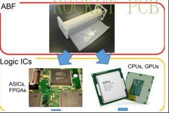
An ABF interfaces an IC with the PCB. Image used courtesy of the Ajinomoto Group
2. ABF Substrate board applications
The AFB substrate consists of multiple layers of microcircuits, known as "building block substrates", which allow for the formation of these miniature components because its surface can be laser-machined and directly copper-plated. Most modern chip makers use ABFs to design smaller components in their CPUs and GPUs.

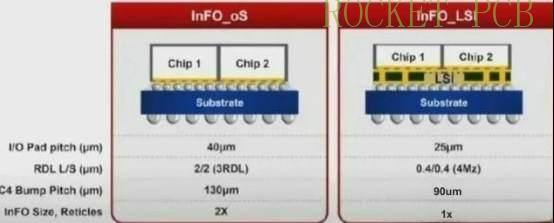
A lower level look at the ABF within a package. Image used courtesy of the Ajinomoto Group
Compared with BT Substrate boards, ABF material can be used for ICs with thinner lines, suitable for high pin count and high message transmission, with higher computing performance, mainly used for CPU, GPU, FPGA, ASIC and other high computing performance chips. ABF substrate matches the semiconductor advanced process to meet the requirements of its thin line and thin line width. Currently, ABF Substrate boards have become the standard for FC-BGA packages.

3. ABF Substrate Board Manufacturer
In the global market, ABF substrates are dominated by a handful of players from Japan, Taiwan China, and South Korea. Major ABF substrate manufacturers include Unimicron, Ibieen,Nanya PCB , Shinko Electric Industries, Kinsus, AT&S, Semco, and Kyocera, with the top eight players accounting for more than 85% share globally. Almost all ABF substrate manufacturers are planning to expand their production capacity in the coming years, and several other companies are planning to enter into the production of ABF substrates due to the high market potential, such as LG Innotek, Shennan Circuit, Shenzhen FastPrint Technology, Access and NCAP China.
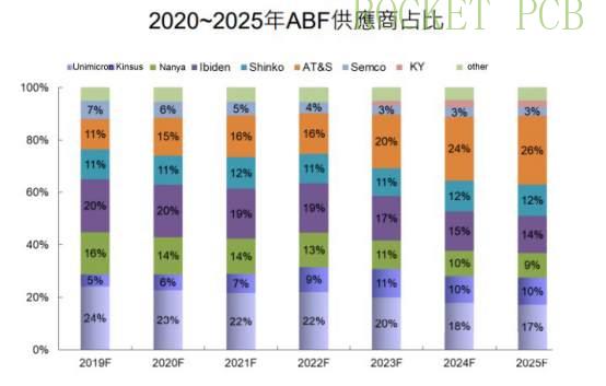
Currently there are seven major suppliers of ABF Substrate boards, the proportion of supply in 2021 are Unimicron 21.6%, Kinsus 7.2%, Nanya PCB 13.5%, Ibiden 19.0%, Shinko 12.1%, AT&S 16.0%, Semco 5.1%. In 2022, except for Semco, the rest of the manufacturers are expanding production.
Proportion of ABF suppliers in 2020~2025

4. Background of the development of ABF Substrate boards
4.1 Advanced Packaging, the "Greatest Hits"
Currently, advanced packaging technologies include FC BGA, FC QFN, 2.5D/3D, WLCSP, Fan-Out, etc. Among them, FCBGA has become the mainstream packaging technology by virtue of its internal FC and external BGA packaging. As a package technology with more applications in ABF Substrate boards, FCBGA has an I/O count of 32~48, and thus has excellent performance and cost advantages. In addition, the I/O count of 2.5D package is also quite high, which is several times higher than that of 2D FC package. While significantly improving the performance of high-level chips, the required ABF Substrate boards also become more complicated.
Taking TSMC's CoWoS technology as an example, since its debut in 2012, this packaging technology has been categorized into CoWoS-S, CoWoS-R, and CoWoS-L according to the different Interposer, with the fifth-generation CoWoS-S now in mass production and the sixth-generation CoWoS-S expected to be mass-produced in 2023. As one of the advanced packaging technologies, CoWoS adopts a large number of high-order ABFs, which are higher than FCBGA in terms of area and number of layers, and the yield is much lower than that of FCBGA, and from this aspect, a large amount of ABF capacity will be consumed in the future.
In addition to TSMC, Intel's Embedded Multi-die Interconnect Bridge (EMIB) technology, released in 2014, has a high I/O count of 250~1000 to increase chip interconnect density and embed the silicon intermediary layer in the ABF to save a large area of silicon intermediary layer. Although this move reduces the cost, it increases the area, number of layers and production difficulty of the ABF, which will consume more ABF capacity. It is understood that Eagle Stream's new platform Sapphire Rapids will be the first Intel Xeon data center product with EMIB + Chiplet, and it is estimated that ABF consumption will be more than 1.4 times that of the Whitley platform.
As a result, the emergence of advanced packaging technology has undoubtedly been a major contributor to the demand for ABF Substrate boards.
4.2 Upgraded Demand in the Server and AI Sector
If advanced packaging technology is a major contributor, then the rise of data centers and artificial intelligence applications is the number one "enabler". At present, in order to meet the needs of HPC, AI, netcom and various infrastructure, whether it is CPU, GPU, netcom chips, or special application chips (ASIC) and other key chips, will accelerate the speed of content upgrading, and then to the large size, high-level number, high-density lines in the direction of the development of the three directions, and such a development trend will inevitably pull up the market for the demand for the ABF Substrate board.
On the one hand, the advanced packaging mentioned above as a major tool to improve chip arithmetic and reduce the average price of the chip, coupled with the rise of data centers and artificial intelligence and other fields of computing power put forward a new requirement, more and more CPU, GPU and other large arithmetic chips began to move towards advanced packaging. So far this year, the most shocking should be the M1 Ultra chip launched by Apple in March.
It is understood that the M1 Ultra uses Apple's customized packaging architecture Ultra Fusion, based on TSMC's InFO-L packaging technology architecture, through the silicon intermediary board connecting the two M1 Max die crystal, to build out the SoC, which can maximize the reduction of the area and improve performance. The InFO-L packaging technology used in the M1 Ultra requires a large area of ABF, twice the area of the M1 Max, and a higher degree of precision than the packaging technology used in previous processors.

In addition to Apple's M1 Ultra chip, NVIDIA server GPU Hopper and Ultra Semiconductor's RDNA 3 PC GPUs will be converted to 2.5D packaging this year, and in April of this year, there were media reports that ASE Group's Advanced Packaging had cut its way into the supply chain of the top U.S. server chip makers.
All signs imply that the advancement of high-computing-power chips to advanced packaging will become the main reason for the growth of demand for ABF Substrate boards. On the other hand, it is the rise of new technologies and applications such as AI, 5G, autonomous driving, and Internet of Things. In terms of the most popular meta-universe before, AR/VR and other headset devices as an important entrance to the future meta-universe, behind the hidden huge chip opportunities, and these chip opportunities will also become a new growth force to promote the growth of the ABF Substrate board market.
5. Analysis of the current status of the ABF Substrate industry
From the global ABF Substrate industry market size, the ABF Substrate market size continues to grow. According to relevant data, the global ABF Substrate industry market size reached USD 4,368 million in 2021, and the market size is expected to reach USD 6,529 million in 2028, with a CAGR of 5.56% for the global ABF Substrate market size from 2022 to 2028.
From the industry supply and demand situation, ABF Substrate board is currently in a situation of short supply, and it is expected that there will still be a supply and demand gap until year 2024. According to the data, the global average monthly demand for ABF Substrate boards will be 185 million pcs in 2019 and will reach 345 million pcs in 2023, with a CAGR of 16.9%. And the global average monthly production capacity of ABF Substrate board will grow at a CAGR of 18.6% from 2019-2023, and the monthly production capacity is expected to reach 331 million pcs in 2023, however, the supply-demand gap has been reduced, but it still can't satisfy the market's demand of 345 million pcs. Tight supply has also led to rising ABF prices, with ABF Substrate board prices increasing by approximately 30%-50% since the second half of 2020.
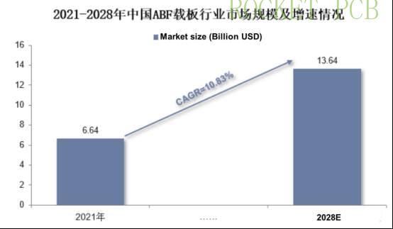
The current supply of ABF Substrate is insufficient, mainland China ABF substrate manufacturers have increased investment, seize the opportunity to seize the global market share of packaging substrates, accelerate the process of domestic substitution. At present, there are Shennan Circuit, FastPrint technology, Zhuhai ACCESS has the expansion of ABF substrate production capacity, Huazheng new material, Nanya new material are making the most critical and the bottle-necked ABF film layer materials. According to data, in recent years, China's regional ABF Substrate board market size is growing faster than the global market size of $664 million in 2021, accounting for about 15.2% of the global market size, is expected to reach $1.364 billion in 2028, when the global share will reach 20.9%.
China’s ABF Substrate Board Industry Market Size and Growth Rate, 2021-2028

6. Future Development Trends of ABF Substrate Board Industry
6.1 ABF Substrate Board Layer and Area Continues to Grow with High Performance Computing (HPC) Demand
At this stage, the number of layers of ABF Substrate board high-end products have fallen in 14-20 layers, the area is 70mmx70mm, and even 100mmx100mm products have been related to the design of the line fine density has gradually entered the 6-7 micron, in 2025 officially entered the 5 micron competition.
6.2 Chiplet Packaging Technology Energizes IC Substrate Board Industry
Currently, Chiplet is a solution of greater interest to a number of leading IC vendors such as AMD, Intel, TSMC and others. According to Omdia's statistics, in 2024, the global market size of processor chips using Chiplet will reach 5.8 billion U.S. dollars, and will reach 57 billion U.S. dollars in 2035, with a compound growth rate of about 23.09%, the rapid growth in the market size of Chiplet processor chips will drive an increased demand for ABF Substrate board. Advanced packaging technology to promote the consumption of ABF Substrate board capacity, the introduction of 2.5/3DIC high-end technology products, the future has the opportunity to enter the mass production stage, is bound to bring greater growth momentum.
7. Summarize
Benefit from 5G, AI cloud computing, big data analysis and other applications to drive the demand for high-performance computing chips, coupled with the "home economy", remote work and other scenarios to promote the CPU, GPU and other LSI chips multiply the amount of FC-BGA substrate demand has increased greatly, the ABF Substrate boom rise. ABF Substrate will be the future of electronics manufacturing.
We must recognize that the position of ABF Substrate boards cannot be shaken in the short term. the supply side of ABF Substrate boards is a game for the few, with extremely high financial and technical barriers. Ajinomoto's ABF substrate capacity is in short supply, which is the root cause of the shortage of ABF Substrate boards.
ABF technical difficulties lie in the ABF substrate and fine line width of the manufacturing process, the technical threshold is high, the key to expanding production is to be able to recruit enough technical personnel, because the ABF Substrate board in addition to the ABF substrate, the high multi-layer, fine-pitch line process requirements are extremely high. For example, the number of high-end ABF Substrate layer has reached as high as 20 layers, line width into the rang of 6μm ~ 7μm, testing the manufacturer's technology research and development and talent reserve capacity. China's mainland IC Substrate industry development has the opportunity to break through the limitations,and then expand their presence on the global stage.
Rocket PCB strives to be the most knowledgeable IC substrate solution provider in the Integrated circuit industry, covering both BT and ABF substrates for Coreless, ETS, FCCSP, FCBGA(BT), and FCBGA(ABF), providing customers with a wide variety of choices.


