Why add PCB break-up tab
When PCB makers make PCB files, we often need to add break-up tab on the unit board or panel. This paper describes the design specifications of common break-up tab.
In the process of PCB design, for some reasons, the distance between the edge of components and the long edge of PCB is less than 5 mm. In order to ensure the efficiency and quality of PCB assembly, the designer should add the break-up tab to the corresponding long edge of PCB. (as shown in Figure 1)
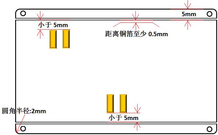
Fig1 break-up tab Specification
When only one long edge is less than 5 mm from the PCB edge, what should be done?
As shown in Fig2, when a long edge has enough distance from the edge of PCB, there is no need to add break-up tab here; especially, no matter how far the short edge is from the edge of PCB, there is no need to process the edge (generally default is this, if the PCB manufacturer has special requirements, according to the circumstances).
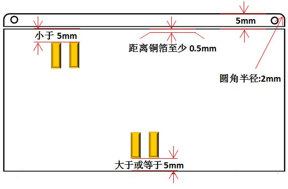
Fig2 Single edge break-up tab
What about adding break-up tab to irregular PCB?
As shown in Figure 3, when there is an irregular long edge for PCB, whether the distance between the component and the edge of PCB is less than 5 mm, Please add break-up tab to the long edge.
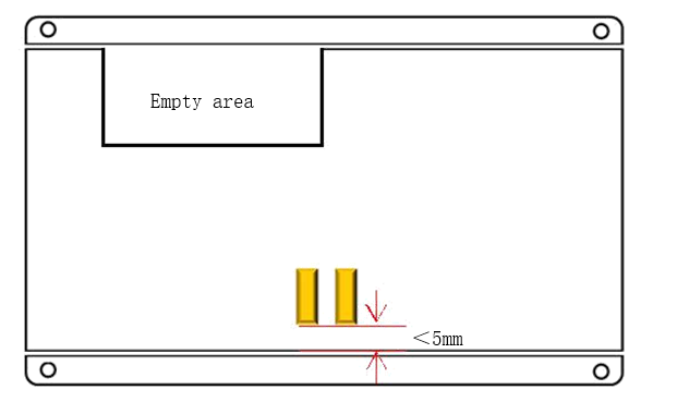
Fig3 Irregular PCB break-up tab
How is the break-up tab handled connected to PCB?
The break-up tab will be removed after the components are soldered on the PCB. In order to remove the break-up tab conveniently, as shown in Figure 4, the designer usually connects the break-up tab to the PCB with V-Cut (V-cut) or stamp hole. Pay attention to the length of figure L, and generally keep more than 1 cm (if there are components with larger quality in the soldering process, L can be lengthened appropriately), so that the PCB connection can withstand enough gravity.
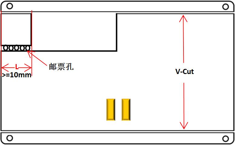
Fig 4 Break-up tab connection
Questions related to V-cut?
When grooving, the designer only needs to place a 2 mm straight line along the edge of PCB as a marker (Reason: the width of the V-cut milling cutter is 2 mm in general); when double-sided V-cut adopted, the depth of V-cut (the sum of two side) should be controlled at about 1/3 of the thickness of the PCB board.
(Specific circumstances can be determined according to the production capacity of PCB manufacturers)
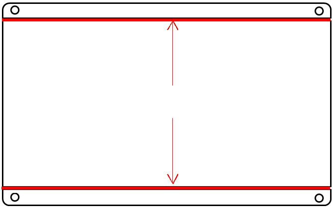
Fig5 V-cut Tag line
Issues related to opening stamp hole
Although stamp holes have stronger endurance than V-grooves, they are prone to burrs in post-processing, so they are not used in general.
If users need to use it, please set it according to the parameters shown in Figure 6
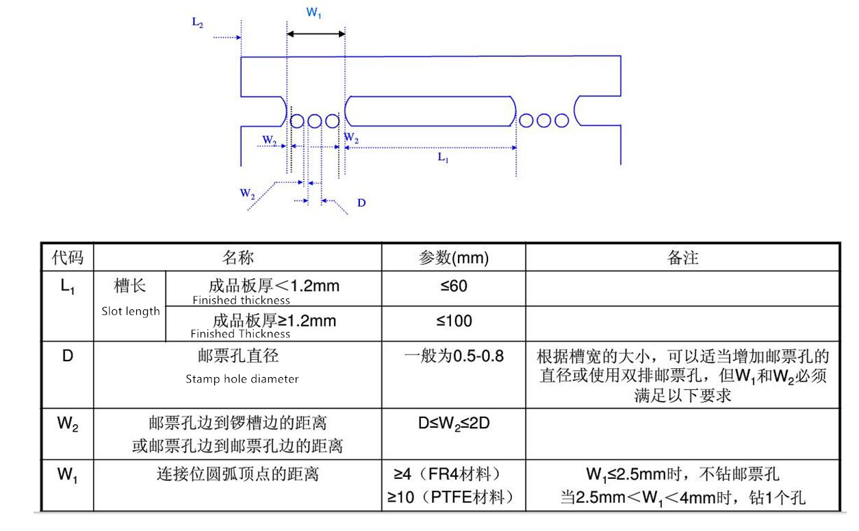
Fig6 Stamp hole specific parameters
This is the design specification for common break-up tab for PCB manufacturing. In general, if the customer designs the outline, PCB maker will draw the outline according to the customer's requirements. Some specially designed PCBs have complex shapes, so they need to be combined with the actual situation to meet the milling path and draw panel route for customer confirmation.


