


Key technology of HDI PCB manufacturing
The successful manufacture of HDI PCB requires special equipment and processes, such as laser drilling, hole filling and electroplating, laser direct imaging and sequential lamination cycle. HDI boards have thinner lines, tighter spacing and tighter rings, and use thinner specialty materials. In order to successfully produce this type of PCB, additional time and significant investment in the manufacturing process and equipment are required.
Compared with traditional PCB technology, HDI PCB has thinner lines and spacing, smaller through holes and capture pads, and higher bonding pad density. HDI PCB is used to reduce size and weight, as well as to enhance the electrical performance of equipment. HDI PCBs are made from microvia and buried vias, and are sequentially laminated with insulation and conductor wiring to achieve higher wiring density. HDI PCB is the best alternative to expensive standard multilayer boards.
With regard to the electrical requirements of high-speed signals, PCB must have some AC characteristics, such as impedance control, high-frequency transmission capability and reducing unnecessary radiation. The structure of stripline and microstrip line must be multi-layer designed. In order to reduce the quality of signal transmission, the insulation materials with low dielectric coefficient and low attenuation rate are used. Due to the miniaturization and array of electronic components, the density of PCB must be increased. With the result of ball grid array, chip scale packaging and direct chip connection assembly methods, PCB has unprecedented high density. Holes less than 150 um in diameter are usually called microvia. It can improve assembly efficiency and space utilization.
HDI PCB has many advantages, such as small size, high speed and high frequency. It is the main component of personal computers, portable computers, mobile phones and personal digital assistants.
Application of HDI board in various fields
Communication smart phones, multi-function phones, video phones, etc
Computers, laptops, supercomputers, tablets, etc
Consumer electronic cameras, digital TV, video recorders, cameras, etc
Automobile radar, navigator and other instruments, infrared analyzer, nuclear magnetic resonance analysis, etc
Aerospace satellites, missiles, black boxes, etc
CC medical equipment electroencephalograph, microelectrode monitor, evoked potential detection system, etc
Industrial control / sensors, printers, remote controls, etc
Via-in-pad (POFV)
Inspired by surface mount technology in the late 1980's, BGA, COB, and CSP were limited to smaller square surface inches. The via in pad process allows the microvia hole to be placed in the surface of a flat pad. The via hole is plated and filled with conductive or non-conductive epoxy resin, then covered and plated so that it is almost invisible. It sounds simple, but it takes an average of eight steps to complete this unique process. Special equipment and trained technicians will pay close attention to the process to achieve the perfect hidden via.
Via hole filling electroplating
There are many different types of via-hole fillers: non-conductive epoxy, conductive epoxy, copper filled, silver filled, and electrochemical plating. All of this will result in the via being buried in a flat pad that will be fully welded like a normal pad. Vias and microvias are drilled, blind or buried, filled, then plated and hidden under the SMT pad. This type of via-hole requires special equipment and is time-consuming. Multiple drilling cycles and controlled depth drilling increase processing time.
When the laser blind hole filling electroplating, the main components of sulfate type electroplating solution commonly used in electroplating hole filling include sulfuric acid, copper sulfate, additives and chloride ions, etc. The aspect ratio of blind hole is generally 3:4-1:1. In order to ensure the effective deposition of Cu2 and reduce the risk of bubbles and cavities in the hole, the system with high copper and low acid is mainly used. Chloride ion is a common anode activator, which can reduce the stress and keep the coating bright and smooth. At the same time, it can inhibit the deposition rate of Cu2 on PCB surface, coordinate with cu3 and improve the reduction rate of Cu2. Chloride ion is usually controlled at about 50 × 10 ℃. Additives mainly refer to carrier, leveling agent and brightener, which can affect the deposition process, control the morphology and properties of the deposition layer, and keep the surface bright, uniform and smooth.
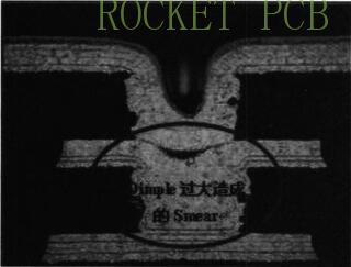
Smear caused by too large dimple in blind hole filling
Through the understanding of the principle and influencing factors of the above-mentioned hole filling electroplating, we know that it is very important to control the liquid medicine parameters and select the appropriate electroplating parameters. Therefore, the vertical continuous plating (VCP) with jet design should be selected for production.
VCP line
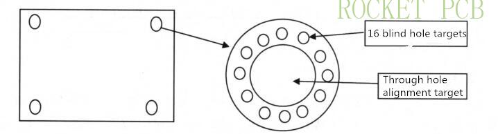
Contraposition and fluctuation
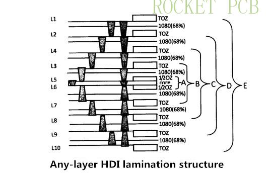
The application of LDI technology can improve the alignment accuracy and reduce the docking deviation in the fabrication of HDI board of any layer. In addition to using LDI technology, alignment target can be designed, alignment mode can be selected and alignment degree can be controlled. The target design is the key to accuracy control, which is often ignored in practical work. Such as 10L any-layer HDI, When selecting single mechanical hole for L5 ~ L6 core plate, attention should be paid to the thickness of stack plate, drilling parameters and quality of drill bit; for other layers, compound targets should be selected for alignment, and 12 ~ 20 target points should be designed at the periphery.
In terms of expansion and shrinkage control, materials should be carefully selected, mainly high stability and high Tg materials: pay attention to engineering design details, optimize graphic design, select small panel design, set prevention coefficient according to test data; optimize process design, strictly control plate parameters, use chemical method to reduce copper; strictly control temperature and humidity of production and storage environment. In the actual work, it will increase the difficulty of control, so it is necessary to classify the board according to the size of the board to reduce the control difficulty.
Laser drilling technology
Drilling the smallest micro via hole (blind hole) can use more technology on the circuit board surface. Using a beam of 20 microns (1 mil) in diameter, this high impact beam can penetrate metal and glass to form tiny through holes.
Blind hole making is the key technology in HDI board manufacturing. Laser drilling technology includes UV laser drilling, CO2 laser drilling and hybrid laser drilling. Among them, the most commonly used is CO2 laser drilling, which has the advantages of low cost and high efficiency. In the aspect of pore size control, due to the low resolution of the pore forming technology, the via diameter is usually greater than 0. 1 mm, while the electroplating hole filling requires that the pore size should not be too large, otherwise the filling effect will be affected. Therefore, the pore size must be controlled at 0.1 mm.
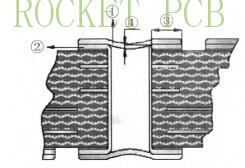
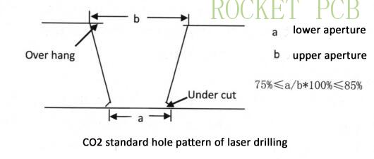
It is difficult to control the core board of L5 ~ L6( 10 layer board). It is also necessary to prevent the bottom copper from being penetrated when controlling the hole diameter and shape. The key to the production of HDI board is the production of core board, which directly affects the success of HDI board production. The main factors affecting the diameter of blind hole are wavelength, laser type and diameter, focusing distance and so on. In addition, when making blind holes, attention should be paid to the quality control, including over ablation, overhanging, side erosion roundness, glass fiber, residual glue at the bottom of the hole, etc. The standard shape should be inverted trapezoid, and the lower hole diameter should be 75% ~ 85% of the upper hole diameter, the hole wall should be linear, the hole diameter should be 90um-125um, one side ≤ 10m, true roundness ≥ 85%, side corrosion ≤ 15m, RCC plate ≤ 10um
The standard hole type control of CO2 laser drilling is shown in the figure, the hole wall is straight, the hole is inverted trapezoid (the lower aperture is 75% ~ 85% of the upper aperture), the aperture is controlled at 90 ~ 125 μm, the true roundness is ≥ 85%, over hang (single side) ≤ 10 μm, FR4 plate under cut ≤ 15 μm, and RCC plate under 10 μm
Laminated material and technology of HDI board
Advanced multilayer technology allows designers to add additional layer pairs in turn to form multilayer PCB. Using a laser drill to create holes in the inner layer can be electroplated, imaged and etched before pressing. This addition process is called sequential build. SBU manufacturing using solid filled via allows for better thermal management, stronger interconnection, and improved board reliability.
Resin coated copper (RCC) is specially developed to solve the problem of poor hole quality, longer drilling time and allowing thinner PCB. RCC has ultra-thin shape and ultra-thin copper foil, and is fixed on the surface with tiny nodules. The thinnest pitch of the material has been chemically treated.
The dry resist is applied to the laminate and still applied to the core using the heating roll method. In this older process, it is now recommended to preheat the material to the required temperature before HDI PCB lamination process. The preheating can better apply the dry resist to the surface of the laminate stably, absorb less heat from the hot roll, and ensure the stable outlet temperature of the laminated product. Consistent inlet and outlet temperatures result in less air trapped under the film. This is very important for the reproduction of thin lines and spacing.
LDI and contact images (dry film coverage)
Imaging with thinner lines and using semiconductor class 100 cleanrooms to process these HDI parts is expensive, but necessary. Finer lines, spacing and loops need more control. Using thinner wires, it is impossible to repair or maintain. The quality of the photo tool, the preparation of the laminate and the imaging parameters are essential for successful processing. The use of clean room air can reduce defects. But dry film resist is still the number one process for all technology plates.
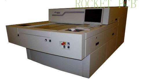
LDI equipment
Because of the cost of laser direct imaging, contact imaging is still widely used. However, for such fine lines and spacing, LDI is a better choice. At present, most factories still use contact imaging in SC100 machine room. With the growth of demand, the demand for laser drilling and laser direct imaging is also growing. All of the HDI production facilities of Rocket PCB use the latest technology to produce this advanced PCB.
Conclusion
There are many production processes of HDI PCB, and the process is complex. In the HDI production, we should first select the process flow, define the key technology of production, control the pore diameter and shape: reasonably mix the composition of electroplating solution; pay attention to the filling rate and sag, ensure the filling effect, strengthen the accuracy and shrinkage control, adopt the LDI technology, design the alignment target, select the alignment mode, carefully select the material, and optimize the project design and process design.


