


Selection Guide for surface treatment of PCB manufacturing
More and more attention has been paid to the environmental problems in PCB production process. In particular, lead and bromine are the most popular topics.
The basic purpose of PCB surface treatment is to ensure good solderability or electrical properties. Because the copper in nature tends to exist in the form of oxide in the air, the original copper is easy to be oxidized, and the oxidation layer of copper is very harmful to soldering, so it is necessary to carry out other treatment for copper.
Now there are many PCB surface treatment processes. The common ones are,
Hot air leveling (HASL)
Organic solderability protector (OSP)
Plating Nickel- hard gold/soft gold
ENIG/immersion gold
Immersion Tin
Immersion silver
Electroless nickel palladium plating (ENEPIG)
PCB surface treatment types
| HASL-LF | Imm-Ni/AU | Imm-Ag | Imm-TIN | OSP | |
| Application ratio | 20% | 10-20% | 10-15% | 5-10% | 20-50% |
| TYPE | Molten solder | E-Ni/ Imm Au | Silver | Tin | Organic |
| SURFACE | Non-Planar | Planar | Planar | Planar | Planar |
| COLOR | Shiny gray | Gold | Silver | Silver | Copper |
| PROCESS | HORIZ | VERTICAL | HORIZ | VERT/HORIZ | HORIZ |
| WIRE BONDABILITY | Aluminum | Aluminum | |||
| NON USED Pad | Protected | Protected | Protected | Unprotected | |
| STORAGE | 1 year | 1 year | 1 year | 9-12months | 6-12 months |
| THICKNESS | >1 um | 3um Ni/0.05um Au | 0.1-0.5 | >1um | 0.2-0.6um |
| REWORK | Average | NO | NO | AVERAGE | EASY |
| ATTACK SOLDER MASK | Little | NO | NO | Yes | |
| HIGHEST TEMP | 270°C | 85°C | 45°C | 60°C | 45°C |
| HIGH TEMIP TIME | 2-5 seconds | 35 minutes | 1 minute | 4-10minutes | 1 Minute |
| CYCLE TIME | 4 minutes | 120 minutes | 10 minutes | 30 minutes | 15 minutes |
| ET TESTING | YES | YES | YES | YES | NO** |
| COST | $$ | $$$$$$ | $$ | $$ | $ |
These processes will be introduced one by one.
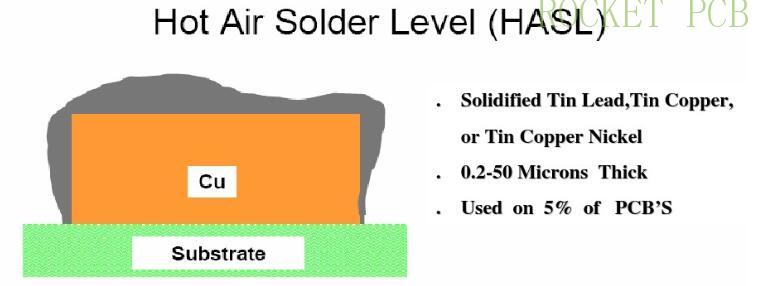
1. Hot air leveling (HASL)/LF-HASL
Hot air leveling, also known as hot air solder leveling (commonly known as HASL), is a process of coating molten tin (lead) solder on the surface of PCB and leveling (blowing) with heated compressed air to form a coating layer which can resist copper oxidation and provide good solderability. Copper tin intermetallic compound is formed between solder and copper in hot air leveling. The thickness of the protective copper surface is about1-2mil.
PCB should sink in the molten solder during hot air leveling; the air knife should blow the liquid solder before the solder solidifies; the air knife can minimize the crescent shape of solder on the copper surface and prevent solder bridging.
Hot air leveling can be divided into vertical type and horizontal type. It is generally considered that the horizontal type is better, and the horizontal hot air leveling coating is relatively uniform, which can realize automatic production.
The general process of hot air leveling process is as follows: Micro etching → preheating → flux coating → tin spraying → cleaning.
Process: when spraying tin on PCB, soak in the molten lead-free solder (about 270 ℃), quickly lift the PCB, and blow the liquid solder from the front and back of the board with hot air knife (temperature 265-270 ℃), so as to make the meniscus solder on the copper surface flatten and prevent solder bridging.
Advantages:
Long storage time
Copper surface is completely wetted (completely covered with tin) after PCB is completed; it is suitable for lead-free welding;
The process is mature, low-cost, suitable for visual inspection and electrical testing.
Disadvantages:
Not suitable for wire bonding;
Limited in SMT due to surface flatness;
Not suitable for contact switch design.
Copper dissolves when tin is sprayed, and the board is subjected to a high temperature. It is not convenient to spray tin on special thick or thin boards.
The coating layer is not flat enough, and it is mainly used for wide wire and large pad board. HDI board is usually not used, which requires high heat resistance of copper clad laminate.
The tin spraying process is dirty and smelly.
It is dangerous to operate under high temperature.
The effect of lead on the environment is limited
There are high requirements for green oil, sheet and laminate bonding, and there are hidden dangers of board bending and board warping. The method to avoid is to use high Tg sheets and PP.
With the development of technology and environmental requirements, lead-free tin spray technology has been widely adopted.
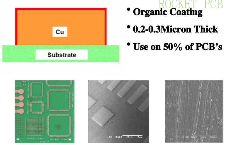
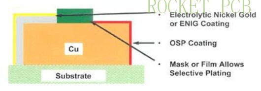
2. Organic solderability protector (OSP)
OSP is a process of copper foil surface treatment of printed circuit board (PCB) which meets the requirements of RoHS directive. OSP is the abbreviation of organic solderability preservation, and English also known as Preflux. In short, OSP is to grow an organic film on a clean bare copper surface by chemical methods. This film has anti-oxidation, heat shock resistance and moisture resistance, which is used to protect the copper surface from further rusting (oxidation or vulcanization, etc. ) in the normal environment. However, in the subsequent welding high temperature, the protective film must be easily removed by the flux, so that the exposed clean copper surface can immediately combine with the molten solder to form a firm solder joint in a very short time. The thickness of OSP is 0. 1-0. 2um, or 0. 2-0. 5um.
At present, the two widely used OSPs are nitrogen-containing organic compounds, namely benzotriazoles and imidazoles. They all adhere well to the bare copper surface, and are copper specific, and will not adhere to the insulation coating, such as solder mask.
The general process is as follows: degreasing, micro etching, pickling, pure water cleaning, organic coating and cleaning. Compared with other processes, the process control is easier.
Advantages:
Simple process, smooth surface, suitable for lead-free soldering and SMT.
Easy to rework, easy to operate, suitable for horizontal line operation.
Suitable for thin lines and fine SM spacing.
The board is suitable for multiple processing (such as OSP + ENIG).
Low cost, environment friendly.
Disadvantages:
Limitation of reflow times (the film will be destroyed after many times of welding, basically no problem for 2 times).
Not suitable for crimping technology, wire bonding.
Because OSP is transparent and non-conductive, it is inconvenient for visual inspection and electrical measurement.
N2 gas protection is required for SMT. SMT rework is not suitable.
The storage condition is high, Not acid resistant, high humidity environment will affect its welding performance
If there is no surface connection functional requirement or storage period limitation, OSP will be the most ideal surface treatment process.
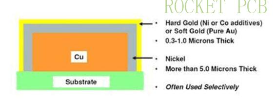
3. Nickel gold plating
Gold plating on PCB is to coat a layer of nickel first and then a layer of gold on the surface of PCB. Nickel plating mainly prevents the diffusion between gold and copper. There are two types of nickel gold plating: soft gold plating (pure gold, gold surface does not look bright) and hard gold plating (surface smooth and hard, wear-resistant, containing cobalt and other elements, gold surface looks brighter). Soft gold is mainly used to make gold wire in chip packaging, while hard gold is mainly used for electrical interconnection of non soldering parts.
Advantages:
Longer storage time > 12 months.
Suitable for contact switch design and gold wire binding.
Suitable for electrical testing
Disadvantages:
High cost, thick gold. Gold Finger Plating requires additional design wire conduction. Because the thickness of gold is not consistent, it may cause the solder joint embrittlement and affect the strength when it is used in welding. The uniformity of electroplating surface. The electroplated nickel gold did not cover the edge of the wire. Not suitable for aluminum wire bonding.
Selective nickel gold+organic coating (picture)
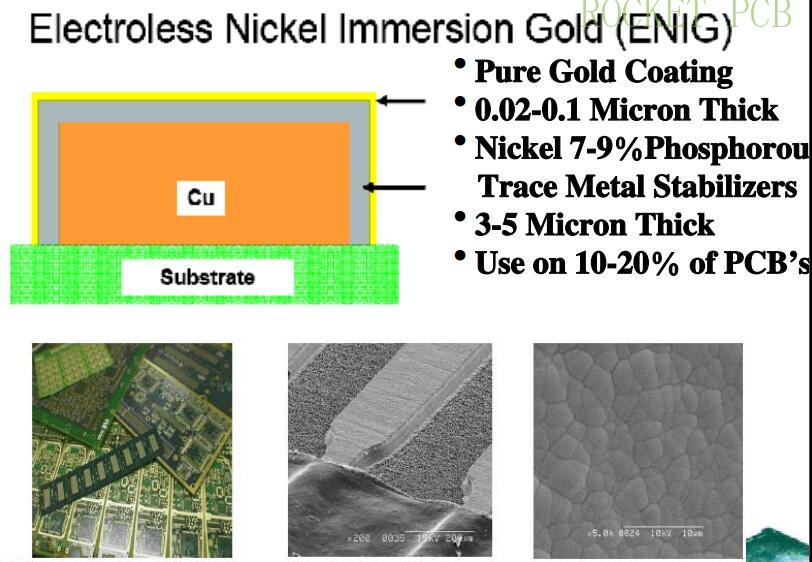
4. Immersion gold&ENIG
The general process is as follows: pickling and cleaning, micro etching, pre leaching, activation, electroless nickel plating and gold leaching. There are six chemical tanks in the process, involving nearly 100 kinds of chemicals, and the process is relatively complex.
Immersion gold is a thick layer of nickel-gold alloy with good electrical properties on the copper surface, which can protect the PCB for a long time. In addition, it also has the tolerance to the environment that other surface treatment processes do not have. In addition, depositing gold can prevent the dissolution of copper, which will benefit lead-free assembly. The thickness of Ni layer is 3-5um and that of Au layer is 0. 02-0. 1um.
Advantages:
Not easy to oxidize, can be stored for a long time, smooth surface, uniform Ni / Au coating, good coplanar. It is suitable for welding thin gap pins and components with small solder joints. PCB with buttons is preferred (such as mobile phone board). Reflow soldering can be repeated many times, which will not reduce the solderability. It can be used as the substrate of cob (chip on board) wire.
Disadvantages:
High cost, poor welding strength, because the use of electroless nickel plating process, easy to have the problem of black disk. The nickel layer will oxidize over time and long-term reliability is a problem.
Black disk effect: it occurs at the interface of Ni and Au, which directly shows the excessive oxidation of Ni. Too much gold will make solder joint brittle and affect reliability.
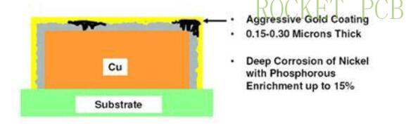
Black disk
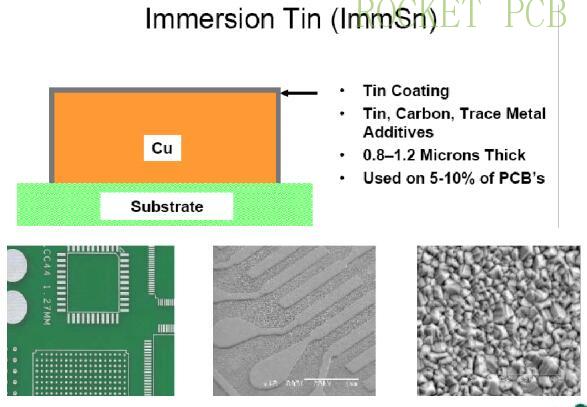
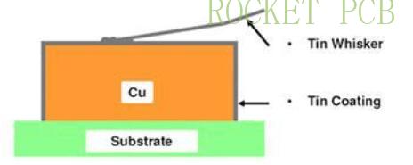
5, Immersion tin
Since all current solder is based on tin, the tin layer can match any type of solder. The tin deposition process can form a flat copper tin intermetallic compound, which makes the deposited tin have the same good solderability as hot air leveling, without the headache flatness problem caused by hot air leveling; there is no diffusion problem between electroless Ni / Au metals, and the copper tin intermetallic compounds can be firmly bonded together. The immersion tin board can not be stored for a long time. It must be assembled according to the sequence of immersion Tin.
Process: degreasing - micro etching - Pickling - pure water washing - tin deposition - cleaning.
Thickness: 1. 0 ± 0. 2 μ M.
Advantages:
Suitable for horizontal production. It is suitable for fine line processing, lead-free welding, especially for crimping technology. Very good flatness, suitable for SMT.
Disadvantages:
(1) The interface compound formed after one welding will become a non weldable surface if it can not withstand multiple welding.
(2) Tin whiskers will be produced and reliability will be affected. Therefore, it is better not to store for more than 6 months.
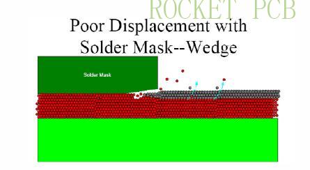
(3) The tin deposition solution is easy to attack the solder mask, which dissolves and discolors the film, and produces reverse corrosion on the copper layer. That is to say, it requires high technology of solder mask.
(4) The temperature of tin deposition is high, ≥ 60 ℃, and it takes ten minutes for 1 micron tin layer.
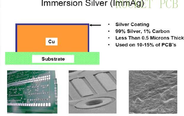
6. Immersion Silver
The process of immersion silver is between organic coating and immersion nickel / gold , which is relatively simple and fast. Even if exposed to hot, wet and polluted environment, silver can still maintain good solderability, but it will lose luster. Immersion Silver does not have the good physical strength of immersion nickel / gold because there is no nickel under the silver layer. The Ag thickness is 0. 1-0. 5um.
Ag ions are prone to electron migration under the action of voltage, so some organic compounds are included in the process of silver precipitation to prevent silver from discoloration and migration.
Advantages:
Simple process, suitable for lead-free soldering, SMT. Very smooth surface, low cost, suitable for very fine lines.
Disadvantages:
High storage conditions, easy to pollute.
Do not store in wet environment, Sensitive to chlorine and sulfur pollution, packaging needs to use sulfur-free paper packaging
Soldering strength is prone to problems (micro cavity problem).
It is easy to appear electromigration and javanni undercutting on copper under solder mask.
7. Immersion nickel palladium gold&ENEPIG
Compared with ENIG, there is more palladium between nickel and gold in ENEPIG. The deposition thickness of Ni is 120 ~ 240uinch (about 3-6um), the thickness of palladium is 4 ~ 20uinch (about 0. 1-0. 5um), and the thickness of gold is 1 ~ 4uinch (about 0. 02 ~ 0. 1um). Palladium can prevent the corrosion phenomenon caused by displacement reaction and make full preparation for gold immersion. Gold is tightly covered with palladium, providing a good contact surface.
Advantages:
Suitable for lead-free soldering. The SMT surface is very flat and suitable. Through holes can also be plated with nickel and gold. Long storage time, storage conditions are not harsh. Suitable for electrical testing. The design of contact switch is suitable. Suitable for aluminum wire binding, suitable for thick board, strong resistance to environmental attack.
Disadvantages:
Palladium is expensive and a scarce resource. At the same time, as the chemical nickel gold, the process control is strict. Due to the late start, there is no large number of applications.
8. Other: Electroplating gold finger (hard gold)
In order to improve the wear resistance of the products and increase the times of inserting and pulling, hard gold is plated.
Comparison of different surface treatments
| LF-HASL | The coating is uneven, mainly suitable for large welding pad and wide line distance. It is not suitable for assembly of fine circuit and fine parts |
| OSP | Uniform coating, flat surface, no contact function, can not be inspected from the appearance, not suitable for multiple reflow. |
| Imm-NI/AU&ENIG | Uniform coating, smooth surface, good contact, good solderability, can wire bonding, can help heat dissipation, and has a certain wear resistance. It is easy to have black disk phenomenon. |
| Imm-Tin | The coating is uniform, the surface is flat, it is aggressive to the solder mask (covering film), and the tin whisker hidden danger is difficult to control. Poor heat resistance, high environmental requirements, easy aging, discoloration |
| Imm-Ag | Uniform coating, flat surface, resistant to multiple assembly operations, with button contact function, can be wired bonding. High environmental requirements, easy aging,discoloration. |
| Electro-Ni/Au | The coating is not uniform, good contact, can be wired bonding, good wear resistance, not suitable for soldering, there is gold brittleness |
| ENEPIG | The coating is uniform and the surface is flat. Palladium is a scarce resource. |
Conclusion
The change of PCB surface treatment process is not very big, but it should be noted that long-term slow change will lead to great changes. With the increasing voice of environmental protection, the PCB surface treatment process will certainly change greatly in the future.


