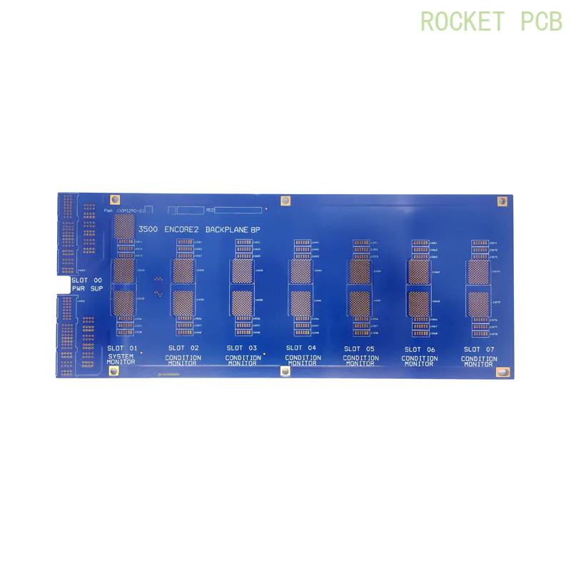
Backplane Application
Backplane applications are very wide, ranging from communication equipment, servers, medical equipment, large-scale machinery, and aviation equipment that need backplane PCB, to computers, servers, and other integrated intelligent electronic devices, also need to organically coordinate various functional modules through the backplane PCB to achieve better system performance.
Features of backplane PCB
The backplane has a lot of distinctive features.
Size
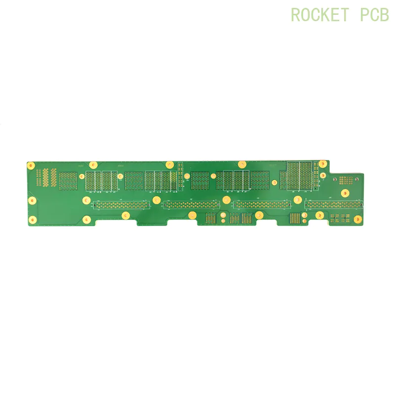
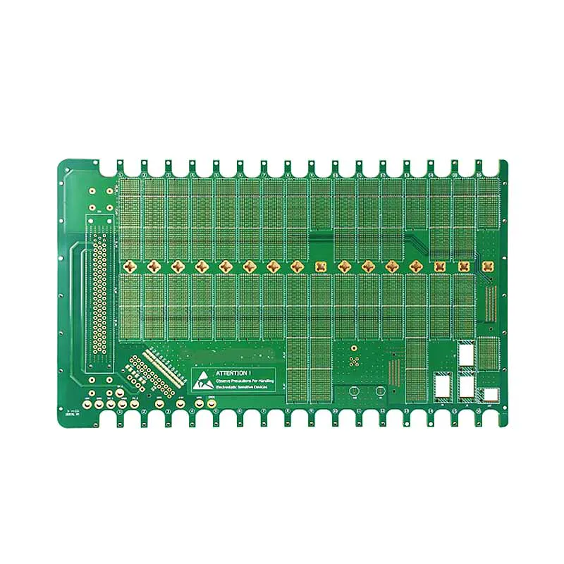
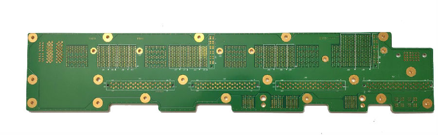
A large part of the backplane is connected to some of the other boards at right angles. This requires that the backplane be much larger than conventional PCBs and that some backplanes even reach the 762mmx1066. 8mm
The number of layers
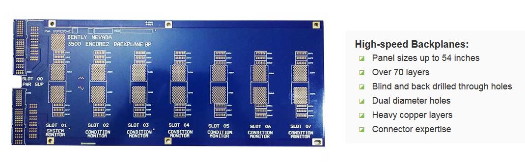
In terms of the most common backplane, its layer is already in the 16~28, this number is much higher than the ordinary PCB
Thickness
From the structure of the backplane itself, in order to be able to withstand more mechanical stress, it has to be designed much thicker than an ordinary PCB. In most cases, the designer has to increase its thickness, and the typical backplane thickness is 2mm-4mm, which can be as thick as 4mm-6mm.
With the continuous development of science and technology, users of bandwidth requirements are becoming more and more stringent, which requires that the design of the backplane to be precise and rigorous enough, the production process of ordinary PCB has been far from meeting the needs of modern production. In order to produce a backplane that meets a variety of conditions, it is necessary to eliminate some of the original conventional equipment and replace it with a hybrid bus structure and assembly technology.
What're the key points of Backplane Technology
In order to achieve such high-performance requirements, PCB manufacturing must face the challenges of strict plate thickness, the board size, number of layers, alignment control, back drilling depth, and stub line. In terms of backplane manufacturing, all the aspects mentioned below are certain key issues. This paper presents the main difficulties encountered in the manufacturing process of backplane PCB and discusses some convenient skills based on the more than ten years of manufacturing experience of Rocket PCB.
1. Alignment control
Due to more and more layers required by users, the alignment between layers becomes very important. The alignment control is the most important manufacturing problem for ultra Multilayer PCB manufacturing, because poor alignment control may lead to short circuits.
The alignment control is affected by many programs and elements, of which cascade is the most important. Tolerance convergence is required for interlayer alignment. The change of plate size makes the convergence more demanding. All layout processes are generated in a certain temperature and humidity-controlled environment. When the exposure equipment is in the same environment, the alignment tolerance of the front and back images of the whole area should be kept at 0. 0125 mm, and a CCD camera should be used to complete the front and back layout alignment. After etching, the inner laminate is perforated using a four-hole system. Through the core plate, the position accuracy is 0. 025mm, and the repeatability is 0. 0125mm. Then the pin is inserted into the perforation to align the etched inner layers and bond the inner layers together. Using this method, the hole can be fully aligned with the etched copperplate to form a solid annular design structure. However, in order to keep the fixed cost of PCB unchanged, the etching copper plate size is required to be smaller, so the interlayer copper plate is required to be better aligned. Fixtures and conveying equipment must be able to transfer large and heavy plates simultaneously.
Tips:
The best composition method is - because it does not cause an impact effect on the core plate.
When pins cannot be used due to certain restrictions, copper iron rivets and short pins are a good choice.
When using a pin Lam stack up, which pin to use is very important. For example, we found that four pins are used to perform better than eight-round pins, which are compatible with the requirements of alignment control.
2. Drilling technology
Due to the thickness of the backplane, the holes may be too short to reach the board. However, too-long drilling tools are often damaged during drilling. In addition, excessive dust may plug holes and cause burrs, which greatly reduces the performance of the backplane PCB.
Tips:
· the CCD method shall be suitable for drilling backplane and CCD marking depending on drilling through X-rays.
· the depth of the borehole can be accurately determined by depth control in a conductive manner.
3. Electroplating capacity
Due to the high thickness of the backplane, the aspect ratio will also be high. In order to ensure that there is enough copper in the hole, if the electroplating is not deep enough, there will be enough copper in the hole, and too much copper will be left at the hole, which will affect the hole diameter, resulting in the incompatibility between the hole diameter and the copper thickness of the hole wall.
Tips:
The pulse plating solution should be compared with the direct current plating solution in terms of electroplating capacity, reliability, and solution stability.
· A new DC plating solution such as EP should be used.
4. ICD analysis
ICD often occurs in the manufacturing process of high-frequency materials, resulting in serious quality risks of electrical connections and long-term reliability. The causes and solutions of ICD should be summarized in order to avoid such problems in the PCB manufacturing process. The reason for the ICD problem is that the resin gel residue left inside the copper layer is not clean enough.
Tips:
The aging degree of the plate should be analyzed.
Control of drilling parameters should be optimized to demonstrate that gel residues have been eliminated.
5. Backdrilling Stub
As far as high-speed signal transmission is concerned, the stub will cause signal distortion or even signal transmission failure. Therefore, the negative impact of stubs on high-speed signal transmission should be clarified. So far, it can be concluded that when the back drill stub length is less than 0.25 mm, the impact on the signal is very small and can be ignored. Therefore, the length of the stub should be controlled within 0.25 mm.
Tips: The length of the short pipe should be controlled within 0. 25 mm to minimize its impact on signal transmission quality.
6. Uniformity of copper plating
In addition to the requirement of uniform plating thickness for drilling holes, the backplane PCB designers generally have different requirements for copper uniformity on the outer surface. Some designs etch very little signal circuitry on the outer layer. On the other hand, in the face of high-speed data rate and impedance control line requirements, it is necessary to set up a near-solid copper sheet in the external layer for the EMC shielding layer. Since the user requires more layers, it is very important to ensure the defect identification and isolation of the inner etching layer before bonding. In order to achieve effective and repeatable control of backplane impedance, etch line width, thickness and tolerance become key indicators. At this time, the AOI method can be used to ensure that the etched copper pattern matches the design data. Using the impedance model, the sensitivity of impedance to line width variation is determined and controlled by setting the line width tolerance on AOI.
Traditionally, passive components are used on the backplane for reliability reasons. However, in order to maintain the fixed cost of an active board, BGA and other active devices are more and more designed on the backplane PCB. Component mounting equipment must be able to accommodate not only smaller capacitors and resistors, but also additional silicon encapsulated components. In addition, the large-scale specification of the backplane requires that the installation equipment bed should be large, and the counterweight backplane can also be shifted with fine position tolerance.
Rocket PCB has unique advantages in backplane manufacturing technology and is the leader of the PCB industry. As China's leading PCB manufacturing service provider, it can handle high-speed and mixed backplane PCB customization services and can make 10G, 25G, 56G, automotive radar hybrid PCB boards.
Design Consideration of High-Speed Backplane PCB
Design considerations for high-speed backplane PCB when the data rate exceeds 1 Gbps, designers must solve new problems in the design of their backplane system. The signal integrity of these backplanes is affected by skin effects, dielectric losses, crosstalk, and ISI. Skin effect is a phenomenon in which most of the current will be concentrated on the outer conductor as the frequency increases.