
English


HDI board is the abbreviation of the high-density interconnector, it is a kind of technology to produce printed circuit boards. It is a circuit board with high distribution density using micro blind and buried hole technology. HDI PCB is a compact product designed for small-capacity users. It adopts modular and parallel design. The product adopts full digital signal processing (DSP) technology and many patent technologies, with the full range of load adaptability and strong short-term overload capacity, and can not consider load power factor and peak factor.
As PCB is not a general terminal product, the definition of the name is a little confusing. For example, the motherboard used for personal computers is called the motherboard rather than the circuit board directly. Although there are circuit boards in the motherboard, they are not the same, so when evaluating the industry, they are not the same. Another example: because the integrated circuit parts are loaded on the circuit board, the news media call it the IC board, but in fact, it is not the same as the printed circuit board.
On the premise that electronic products tend to be multi-functional and complex, the contact distance of integrated circuit components will be reduced, and the speed of signal transmission will be relatively increased, followed by the increase in the number of wiring, the length of wiring between points will be locally shortened, which requires the application of high-density line configuration and micro-via technology to achieve the goal. Wiring and bridging are basically difficult to achieve for single and double-sided boards, so the boards will move towards multi-layer, and because of the continuous increase of signal lines, more power layers and ground layers are the necessary means for design, which makes the multilayer printed circuit board more common.
For the electrical requirements of high-speed signals, the circuit board must provide impedance control with AC characteristics, high-frequency transmission capacity, reducing unnecessary radiation (EMI), etc. With the structure of stripline and microstrip, multi-layer design becomes necessary. In order to reduce the quality of signal transmission, insulating materials with low dielectric coefficient and low attenuation rate will be used. In order to match the miniaturization of an array of electronic components, the density of the circuit board will be continuously increased to meet the demand. With the appearance of BGA (ball grid array), CSP (chip scale package), DCA (direct chip attachment), and other assembly methods, the printed circuit board is pushed to an unprecedented high-density state.
Where the hole diameter less than 150um is known in the industry as Microvia, the circuit made by the micro-hole geometry technology can improve the efficiency of assembly, space utilization, etc., and it is also necessary for the miniaturization of electronic products.
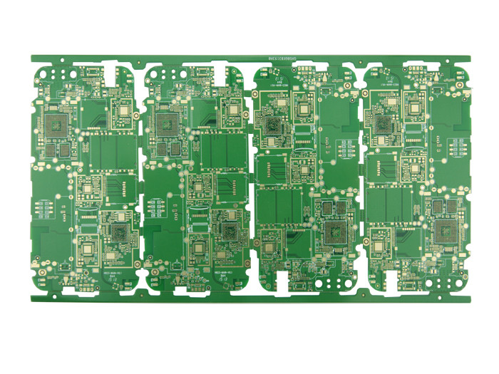
Electronic design not only improves the performance of the whole machine but also reduces its size. From mobile phones to small portable products of smart weapons, "small" is the eternal pursuit. High-density integration (HDI) technology can make the end product design more miniaturized and meet the higher standards of electronic performance and efficiency. HDI is widely used in mobile phones, digital cameras, MP3, MP4, notebook computers, automotive electronics, and other digital products, among which mobile phones are the most widely used. HDI board is generally manufactured by the build-up method. The more the number of layers, the higher the technical level of the board. The common HDI board is basically one-time stacking, and the high-level HDI adopts two or more times stacking technology, and at the same time, advanced PCB technologies such as stacking holes, electroplating filling holes, laser direct drilling are used. High-level HDI board is mainly used in mobile phones, advanced digital cameras, IC substrate PCB, etc.
Insufficient capacity of domestic HDI board
In recent years, the global production situation of the HDI board has changed significantly: most of the HDI production capacity of major PCB manufacturers in Europe and the United States has shifted to Asia. Asia, especially China, has become the main supplier of HDI boards in the world. From the situation of major PCB manufacturers, the existing capacity of domestic major HDI manufacturers is less than 2% of the global total demand. Although some manufacturers have made investments to expand production, overall speaking, the capacity growth of domestic HDI still cannot meet the demand of rapid growth. HDI board market segmentation is obvious, the resources of powerful HDI PCB manufacturers are relatively concentrated. Rocket PCB is one of them, and has rich manufacturing experience in manufacturing high-stage, multi-layer HDI boards, accumulated in the field of HDI for many years, welcome your inquiry!
QUICK LINKS
CONTACT US
Office: (+86) 755 23040566
Tel: (+86) 158 9965 5195
E-mail: sales@rocket-pcb.com
Skype: Hans@Rocket-PCB
Whatsapp: 86 1589965 5195
Office Address: 301 Building/B, Huafeng Digital Technology Industrial Park, Chaoyang Ro, Yanchuan, Songgang,518105 Shenzhen, China.
Plant ADD.: No 69, Lianfeng North Road, Xianxi Area, ChangAn Town, Dongguan, China.


