


How to cope with the challenges of high speed, high integration and high frequency in PCB testing
With the rapid development of cutting-edge technologies such as 5G/6G, artificial intelligence, and smart wearables, electronic products have an increasingly strong demand for high performance, high frequency, and high computing power. As a bridge that carries electronic components and connects circuits, printed circuit boards (PCBs) have ushered in a spurt in demand. As a basic component of electronic equipment, PCBs have increasingly high requirements for high frequency and high computing power. High-frequency signals, complex signal integrity requirements, and higher integration require PCB design and manufacturing to have higher technical content. Therefore, how to effectively test the physical layer of PCBs, especially in high-frequency and high-computing power application scenarios, has become a key link in the development and production of electronic products.
This article will start with three key parameter tests: the basic S parameters such as insertion loss and return loss of PCB single-ended and differential traces; time domain impedance TDR and various indicator tests related to signal integrity (such as FEXT, NEXT, PS_Crosstalk, ICR, ICN, Jitter, differential pair delay, eye diagram, etc.); dielectric properties of PCB materials, such as dielectric constant (Dk)/dielectric loss (Df) and other material parameters. These aspects will discuss in detail the importance and methods of PCB testing when dealing with high-frequency and high-computing challenges.
Testing of basic S parameters such as insertion loss and return loss of PCB single-ended and differential traces
(1). Definition of insertion loss and return loss
In high-speed or high-frequency circuits, the transmission quality of signals is directly related to the performance of the system, and insertion loss and return loss are important parameters that reflect the quality of signal transmission. By testing these parameters, we can better evaluate the advantages and disadvantages of PCB design and materials.
Return loss: also known as reflection loss. Return loss is a parameter that represents the signal reflection performance. Return loss describes the portion of the incident power that is reflected back to the source. For example, if 1mW (0dBm) of power is injected into an amplifier and 10% of it is reflected (bounced) back, the return loss is -10dB. Mathematically, the return loss is -10 lg [(reflected power)/(incident power)]. Return loss is usually specified at both the input and output.
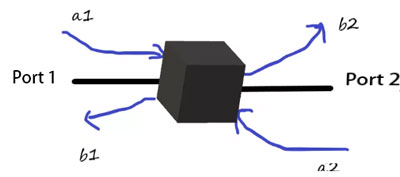
Insertion loss: Insertion loss is the signal loss, usually referred to as attenuation, caused by inserting a cable or component between the transmitter and the receiver. This is shown in Figure 1 below. Insertion loss is expressed in decibels (dB) corresponding to the received signal level. (The smaller the better) Refers to the loss of load power caused by the insertion of a component or device somewhere in the transmission system. It is expressed as the ratio of the power received on the load before the component or device is inserted to the power received on the same load after the insertion in decibels.
(2). How to test
In PCB design, especially in high-frequency applications, each component and connector in the signal transmission path will cause a certain amount of signal loss. Therefore, the test of insertion loss and return loss is very critical. These parameters are usually tested using a network analyzer (Network Analyzer), which can accurately measure S parameters (including insertion loss and return loss) in different frequency bands. Among them, the S11 parameter (reflection loss) and the S21 parameter (insertion loss) are commonly used test indicators.
Insertion loss test: Connect the network analyzer to the signal source and the signal receiving end, and set the appropriate frequency range to measure the loss of the signal propagating in the PCB board.
Return loss test: Also use a network analyzer to measure the reflected signal between the signal source and the receiving end to obtain the return loss.
(3). Importance of testing
Testing insertion loss and return loss is very important for high-frequency PCB design. Especially in high-speed signal transmission circuits, excessive insertion loss and return loss will cause signal attenuation and reflection, affecting the signal transmission quality, thereby causing system performance degradation and even data errors.
In a system with good port matching, insertion loss is mainly caused by the resistive materials of the device. The loss caused by these resistive materials will be converted into heat. The conversion into heat sometimes gives engineers a headache. Because heat is so terrible, almost all electronic devices have a temperature range in which they can work normally. When this temperature is exceeded, they will not work properly. Working in a high temperature environment for a long time will accelerate the aging rate of the device and make it more susceptible to damage.
1. Time Domain Reflectometry (TDR) and signal integrity related tests
(1). Time Domain Reflectometry (TDR) test
Time Domain Reflectometry (TDR) test is a common method for evaluating the impedance characteristics of PCB signal transmission lines. Impedance matching is one of the key factors in high-speed signal transmission. Impedance mismatch will cause signal reflection, thereby affecting the quality of the signal, resulting in bit errors or transmission failures.
TDR testing sends a pulse signal to the PCB circuit and then measures the time it takes for the signal to reflect. By changing the reflection time, it can be determined whether there is an impedance mismatch in the circuit, helping designers find problems and optimize them. TDR testing is usually done with an oscilloscope and a TDR probe.
(2) Signal integrity test
Signal integrity (SI) refers to whether the signal transmission in the PCB can maintain its shape and quality without being affected by noise, distortion or delay. Signal integrity testing includes several important indicators, such as: ·
A. Crosstalk: Crosstalk is divided into near-end crosstalk (NEXT) and far-end crosstalk (FEXT), which respectively represent the mutual interference of signals on adjacent signal paths. Excessive crosstalk will cause mutual interference between signals and reduce the stability of the system. ·
B. Jitter: Jitter refers to small fluctuations in signal timing. Excessive jitter will cause data errors and transmission failures.
C. Eye diagram: Eye diagram is a way to observe the signal waveform through an oscilloscope, which can intuitively reflect the quality of the signal, especially its jitter and distortion.
(3). How to test
Signal integrity testing is mainly done through oscilloscopes, signal analyzers and special test software. Common test methods include:
A. NEXT/FEXT test: Analyze the crosstalk between signals through differential signal channels.
B. Jitter analysis: Use an oscilloscope to measure the timing fluctuations of the signal.
C. Eye diagram test: The oscilloscope forms an eye diagram by superimposing multiple signal waveforms to evaluate the integrity of the signal.
(4). Importance of testing
Time domain impedance and signal integrity are the basis for ensuring the normal operation of high-speed PCBs. Problems such as signal reflection, crosstalk and jitter will directly affect the performance of the circuit, resulting in data transmission errors or system crashes. Therefore, time domain impedance TDR testing and signal integrity testing are essential testing methods in the development of high-frequency PCBs.
2. Testing of dielectric properties of PCB board materials and material parameters
(1). Dielectric constant (Dk) and dielectric loss (Df)
In high-frequency PCBs, the dielectric properties of materials have an important influence on signal transmission. **Dielectric constant (Dk) is a physical quantity that describes the material's ability to respond to an electric field, while dielectric loss (Df)** indicates the degree to which a material attenuates a signal. In high-speed, high-frequency applications, the dielectric constant and dielectric loss of a material directly affect the propagation speed and loss of the signal.
(2). Test method
The dielectric constant and dielectric loss of a material are usually measured by a dielectric tester (such as a network analyzer). By analyzing the S parameters of the PCB material, the Dk and Df values of the material can be obtained.
(3). Importance of testing
For high-speed PCBs, the dielectric properties of the material are crucial. A higher Dk value means a slower signal propagation speed, while a higher Df value results in greater signal attenuation. When designing high-frequency circuits, it is crucial to choose the right material.
3. Conclusion
With the rapid development of technologies such as 5G/6G and artificial intelligence, PCBs, as the basic components of electronic devices, have increasingly higher requirements for high frequency and high computing power. In response to this challenge, physical layer testing of PCBs is particularly important. By testing key parameters such as insertion loss, return loss, time domain impedance, signal integrity and material dielectric properties, designers can optimize PCB design and ensure the stability and reliability of signal transmission. Facing future challenges, further improving and enhancing PCB testing technology, especially in high-frequency and high-computing applications, will be the key to improving the performance and reliability of electronic products.


