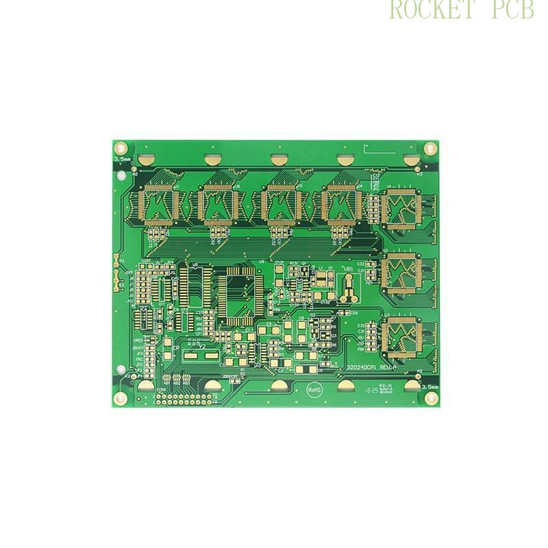
Design and EMC analysis of IoT device PCB
1.Electromagnetic compatibility
Electromagnetic compatibility (EMC) refers to the ability of equipment or systems to work normally in the electromagnetic environment and not to constitute an unbearable electromagnetic disturbance to anything in the environment, which mainly contains two aspects: electromagnetic radiation and anti-interference ability.
Electromagnetic compatibility (EMC) is an important indicator to ensure the reliability and safety and stability of information system equipment, and is also a key technical issue that must be solved in the process of equipment development. Its performance is one of the various safety certifications that must be obtained for electronic and electrical products in major countries and regions around the world. According to IEC/CISPR international standards, EMC design mainly refers to the suppression and protection of electromagnetic interference (EMI).
2.PCB electromagnetic interference analysis
The printed circuit board (PCB) is the platform on which the system circuit works, and its stability determines the characteristics and stability of the circuit work. Currently, with the consumer electronics, industrial electronics design thinking of high-speed, high integration development, according to the international semiconductor technology development blueprint predicts that in 2022 the chip on the clock frequency will increase to 14.3GHz feature size will develop to 11.3mm, due to the increasing clock operating frequency, system speed and circuit integration, PCB internal module signal crosstalk, external electromagnetic signal interference Become a constraint that affects the stability and reliability of the system.
Among the causes of electromagnetic interference is mainly divided into two categories.
(1) PCB board wiring spacing is small, parasitic coupling between the signal lines, and then generate interference. In addition, with the introduction of high-frequency signal modules, the common mode radiation generated by the imbalance between the alignments will also generate interference.
(2) Due to the wiring process, the PCB board has overholes, right-angle bends, bonding lines, etc. These discontinuous structures lead to signal crosstalk, reflection, or the introduction of noise.
In addition, the mutual interference between antennas, antennas and other electronic equipment is also more complex, and may affect the normal operation of antennas and other equipment. Therefore, the EMC analysis and design of the PCB is particularly important.
By introducing EMC design in the PCB design period, the system can be modeled and analyzed by software simulation to find the source of EMI, visualize the simulation results, and do the relevant EMC processing to reduce the system EMI. The earlier the EMC design is introduced, the lower the cost will be.

3.IOT system PCB board EMC design method
IoT system, according to the different service rates, there are differences in the selection of communication modules. For high-speed services, LTECAT-4 modules are commonly used, CAT-1 and eMTC modules are commonly used for low-speed services, and NB-IoT modules are commonly used for low-speed services. Therefore, the signal distribution and power distribution in the circuit need to be taken into account in the EMC design of the PCB of the IoT system for EMC optimization.
3.1 Layout design optimization
(1) According to the system function and signal layout position, IOT communication module and clock module are high-speed devices, should be laid out separately to prevent interference between modules; shielding magnetic components, CPU clock and sensitive devices to maintain a certain distance.
(2) system clock module near its corresponding ground, forming an effective backflow.
(3) power supply part of the optimization program: to prevent digital signals affecting high-frequency analog devices, the analog power supply and digital power supply are separated; to prevent the power line spike current, the formation of noise interference, for the use of power class integrated chip installation decoupling capacitors.
(4) Ground part of the optimization program: decoupling capacitors are added between the ground and power lines) to suppress the radiation current generated on the power lines.
3.2 Wiring design optimization
(1) When wiring, the upper and lower signal line layers are perpendicular to each other as much as possible to avoid the parasitic capacitance caused by parallel lines.
(2) PCB alignment using 45 ° corner, to avoid the signal loss brought about by 90 ° corner alignment.
(3) power line optimization program: according to the power supply voltage provided by the different line width design has some differences, and make the signal direction consistent with its alignment direction, to improve the noise immunity.
(4) Ground line optimization program: ground line using a larger line width to improve the current carrying capacity and reduce parasitic inductance. Cut the ground loop, set up a tic-tac structure, and connect it with filter holes to reduce the antenna effect of the loop.
(5) In order to reduce the radiation, the high frequency signal line should form a loop and reduce the signal line punching.
3.3 Decoupling capacitor
The decoupling capacitor has a bypass effect on electromagnetic interference, but when the circuit signal and work frequency reach GHz, the decoupling capacitor will produce parasitic inductance, which affects the role of decoupling capacitor. Therefore, the design can be optimized from the following aspects.
(1) Punching holes near the decoupling capacitor and connecting it to the power and ground layers of the PCB board (as shown in Figure 1) can effectively reduce the system parasitic inductance.
(2) Place high-frequency decoupling capacitors on the back of the PCB and medium-frequency decoupling capacitors on the front, and place the high-frequency decoupling capacitors as close as possible to the corresponding power supply pins, so as to reduce the current loop area and enhance the decoupling effect.
3.4 Other optimization design
The clock crystal is placed as close to the microprocessor as possible.
A better performance FR-4 board is used, which has a loss angle of only 0.02 at UHF.
4. Conclusion
By optimizing the PCB layout and wiring and increasing the decoupling capacitor, it has certain reference and significance for PCB design rationality and board-level signal integrity.


