


2025 TYPE-C interface new gameplay-desktop display connection interface
With the continuous advancement of technology, traditional desktop monitors can no longer meet the pursuit of modern people for efficient office and ultimate entertainment experience. Against this background, the new TYPE-C interface desktop monitor came into being, leading the new trend of future office and entertainment with its unique functions and design.
Traditional desktop monitors mostly use USB interfaces. USB Type-C (USB-C) is a universal connection standard for device connection and charging. As the latest development of the USB interface, it includes reversible plug direction, higher data transfer rate and power output capability. In addition, USB Type-C can transmit audio and video signals and is compatible with various accessories such as monitors, external storage devices and chargers. Therefore, compared with traditional USB interfaces, USB Type-C interfaces have more advantages.
The USB Type-C (USB-C) interface cable has video transmission function and has made major breakthroughs in charging technology. It cleverly converts the DC power of the monitor into PD protocol to provide power support for connected HOST devices such as laptops and Nintendo. This reverse 100W charging technology not only solves the trouble of users carrying multiple chargers, but also improves charging efficiency and safety, keeps the device at a low temperature while charging, and extends the battery life.
PCB design requirements for TYPE-C interface
In PCB design, the design requirements and considerations of the TYPE-C interface are very important to ensure signal integrity, electrical performance, and reliability.
Unlike traditional USB interfaces, USB Type-C can be inserted in any direction without worrying about the direction. USB Type-C supports higher data transfer rates, reaching the speed of USB 3.1 and Thunderbolt 3, for fast file transfer and video playback. USB Type-C can transmit audio and video signals and supports a variety of accessories such as monitors, external storage devices, and chargers.
Signal Icon
The USB Type-C connector has 24 pins. The two images below show the pinout of a USB Type-C receptacle and plug, respectively.
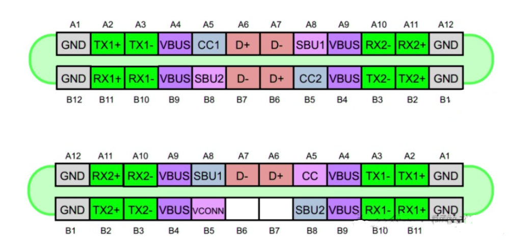
The USB Type-C connector has 24 pins. The two figures below show the pins of the USB Type-C receptacle and plug, respectively.
1.USB Type-C layout design
● ESD and common-mode inductor components should be placed near the Type C interface in the following order: ESD → common-mode inductor → capacitor. Keep a certain distance from the Type C to consider the situation after welding.
● The coupling capacitor of the TX signal line should be placed near the interface, while the coupling capacitor of the RX signal line is placed at the device end.

2. Interface wiring and signal integrity
Differential signal pair (such as TX/RX pair) wiring:
The two signal lines of the differential pair (such as DP/DM, TX+/TX-) need to be wired with equal length, and the length difference is preferably controlled within 5 mil.
The differential impedance is designed to be 90Ω±10%.
Keep the spacing between differential pairs constant to avoid signal crosstalk.
Trace length control:
High-speed signal (such as USB3.1, USB4.0) routing should be as short as possible, and the recommended total length is less than 50 mm.
The length difference of different signal paths should be as small as possible to reduce timing deviation.
Via design:
High-speed signals should avoid using vias as much as possible. If vias must be used, minimize the number of vias and use blind/buried vias.
Place ground vias near vias to reduce impedance mismatch problems.
Interlayer wiring reference ground:
High-speed signal routing needs to have a continuous reference ground plane to avoid crossing the reference plane or breaking the reference plane.
3. Power supply and grounding design
Vbus power supply design:
Vbus power supply design needs to ensure that it can provide sufficient current to meet the requirements of USB PD (Power Delivery).
The power trace width should be calculated according to the current demand, and can be designed according to the standard of 1 A/1 mm.
Place appropriate decoupling capacitors between Vbus and GND, and the recommended values are 0.1 µF, 1 µF, and 10 µF.
GND design:
Provide a good ground plane to ensure signal integrity and power stability.
The metal part of the TYPE-C shell needs to be connected to the GND on the PCB through a low-impedance path to reduce electromagnetic interference (EMI).
3. Signal protection and EMC design
ESD protection circuit:
Add ESD protection devices (such as TVS diodes) on signal lines such as D+/D-, TX+/TX-, CC1/CC2.
The selection of TVS diodes must meet the requirements of high-speed signal transmission and have low capacitance (such as **<0.5 pF**).
Filtering and decoupling:
Add filter capacitors between the power line (Vbus) and the ground line (GND).
Common-mode inductors can be added to high-speed signal traces to suppress differential-mode noise and common-mode noise.
Shielding and grounding:
The metal shell of the TYPE-C interface needs to be grounded.
If the environment has strong EMI/EMC requirements, you can consider designing a shielding layer or shielding shell on the PCB board.
4. CC pin design
CC pin function:
The CC1 and CC2 pins of TYPE-C are responsible for role identification (UFP/DFP/DRP) and current detection.
CC pins need to be connected to resistors (such as Rp, Rd or Ra) to support different working modes and power requirements.
CC signal line traces should be kept short and wide to avoid coupling to other high-speed signal lines.
5. PCB stacking and number of layers
TYPE-C interfaces are usually used for high-speed signal design, and 4 or more layers of PCB are recommended:
Top layer (signal layer): used for TYPE-C interface and key signal routing.
Second layer (ground layer): provides continuous reference ground.
Third layer (power layer): used for power distribution such as Vbus.
Bottom layer (signal layer): other signal traces or backup designs.
6. Mechanical dimensions and installation
Ensure that the mechanical dimensions of the TYPE-C interface match the package design specifications to avoid installation stress affecting solder joint reliability.
The pad design of the TYPE-C interface must comply with IPC standards, and the pad size and position must be accurate to avoid cold soldering or false soldering.
By strictly following these PCB design requirements, the reliability and performance of the TYPE-C interface in actual applications can be ensured.


