


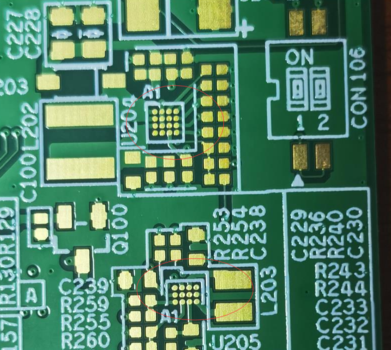
The improvement of signal speed, PCB function density and PCB layer thickness increases the challenges related to PCB design, especially in signal integrity. These limitations force chip manufacturers to produce fine pitch chips (BGA, QFN, flip chip. . . ), while PCB designers combine via in pad (VIP) plating (VIPPO) structure with traditional design (such as dog bone trace, micro via hole, skip via hole and pad with trace to achieve distributability and signal integrity requirements.
What is via in pad?
The last through-hole filling type in IPC-4761 is called Via In Pad. VIP mainly refers to the situation that the through-hole is completely placed in the pad of surface mount device (SMD). Many PCB designers find that they make more use of this via in pad manufacturing process than ever before. As the BGA package becomes smaller and smaller, it becomes more and more difficult to escape the wiring.
When the microvia is placed on the pad to be welded (via in the pad), the hole should be filled. Through holes may be filled and plated with copper or filled with copper to produce an acceptable weldable surface. If the through hole is not filled, the space of the micro through hole will "steal" solder from the expected solder joint. Air trapped after using solder paste may also exhaust gas during reflow assembly and create voids in solder joints.
The emergence and wide use of devices or products with finer spacing and the requirements for smaller PCB have brought new challenges. The exciting solution to these challenges uses a new but common PCB manufacturing technology with a readme name of "via in pad".
Vias in the pad help to reduce inductance, increase density and adopt finer spacing array packaging. Through hole in pad method a through hole is placed directly below the contact pad of the device. This allows higher component density and improved cabling.
Compared with the use of blind holes or buried holes, pad filling holes is a method to achieve medium density at medium cost. Some key advantages of using through holes in pad technology are:
Fan out fine pitch (less than 3 million) BGA
Meet the placement requirements of close arrangement
Better thermal management
Overcome high speed design (HSD) problems and limitations, i. e. low inductance
Through hole plugs are not required for component locations
Provide a flat, coplanar surface for component connections
However, this technology has some disadvantages. The most prominent is the cost impact associated with the adoption of new technologies. PCB manufacturers and suppliers have identified two main cost drivers related to pad via technology: additional HDI PCB manufacturing process complexity and the cost of base materials for conductive filling.
Specifically, pad through hole technology adds 8 to 10 steps to the PCB manufacturing process, and the through hole filling cost is a function of the through hole size and the number of actual through hole instances in any given design. However, the reduction in the number of layers achieved by using through holes in pad technology compensates for the increased costs associated with the process.

Via-in-pad filling or not filling?
If the via in the pad is not filled, the assembly plate may lack some BGA ball to plate connections. If you place vias in BGA pads, your only option is to fill and electroplate vias in the PCB manufacturer.
If you place vias between pads, there are two options. You can place a solder dam on a short path between the pad and the opening. This will prevent solder paste migration. Another better option is to plug the through hole with a solder mask. If any solder mask is too thin or falls off, this will provide some additional protection. Just make sure to cover these things on the soldering surface. If they are covered on the component surface, the solder paste will still spread on the trace and partially enter the through hole. This still puts electrical and mechanical connections at risk.
Solder mask fill or epoxy fill?
When forming via holes in the pad, the solder mask layer cannot be used to fill the vias (microvias) in the pad, because the BGA pad needs to be windowed and cannot be covered with solder mask ink. The solder mask plug hole is easy to cause oil explosion, that is, there are ink rings on the pad and tin beads in the hole. When some PCB boards use solder mask to fill vias, the nearby through holes may suck some solder paste from the pad, so some spacing is required, usually 4mil. Therefore, when the through hole is located inside the pad, this is certainly a larger problem. In this case, Rocket's PCB production team will selectively fill the vias with epoxy resin material instead of using solder mask layer before applying surface treatment, which requires some additional cost and delivery time compared with standard vias.
Conductive or non-conductive epoxy resin filling?
Epoxy resin is usually a non-conductive material, because the conductive material expands faster when heated, which will be troublesome in the reflow soldering process. The non-conductive filler will not hinder the ability of the through hole to conduct current, because the hole wall is still plated with copper like any other through hole. Conductive epoxy resin can also be used when the through hole must transfer a large amount of current or heat through the PCB. When the through holes in the pad are plated through and then filled with conductive or non-conductive epoxy blocking ink, the epoxy ink is then planarized to create a flat surface and plated to obtain fully filled and covered through holes in the pad.
When you send an inquiry with PCB design files to obtain a quotation, it is helpful to note whether there are any vias in the component pad. The pricing and lead time you see in the quotation will take these factors into account, and our CAM engineers can help you determine in advance whether any type of material needs to be filled for a specific via on the circuit board.
Manufacturing process of Via In Pad
Via in pad technology has proved to be a good technology, which can save space and layout PCB at the same time, so as to allow more dense PCB. Not all PCB manufacturers can make via-in-pad during pad manufacturing like Rocket PCB. Here, we list the main via in pad manufacturing process of through-hole PCB, as shown below.
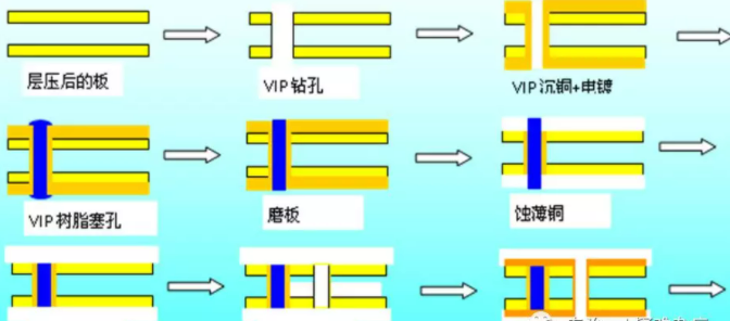
You may find that this is a through hole epoxy filling process for through-hole boards. Yes, but similar. In the microvias in the pad process, the required selective microvias need to be completely filled with epoxy ink, and then planarized and plated to obtain an invisible covered microporous surface. We call it POFV process or VIPPO process.
VIP routing can be realized by overcoming some complexity in manufacturing. Manufacturers will have to eliminate surface protrusions to complicate the process required to connect components such as BGA, as follows:
The manufacturer must create and fill additional through holes for this type of wiring and add new steps in the manufacturing process, including drilling additional holes and electroplating through holes with conductive materials such as copper. Later, fill the through holes with epoxy resin and cover them with copper.
The capped through holes are sometimes easy to deflate. Outgassing or degassing refers to the steam released due to the thermal expansion of the gas. Gas is the result of changing from liquid to steam due to heating during soldering. Outgassing causes voids to form in the solder joint because bubbles move upward through the through hole.
For more questions about the design guide and processing technology of the via-in-pad, please contact Rocket PCB, we will answer you at any time.


