


PCB manufacturing process
Material introduction
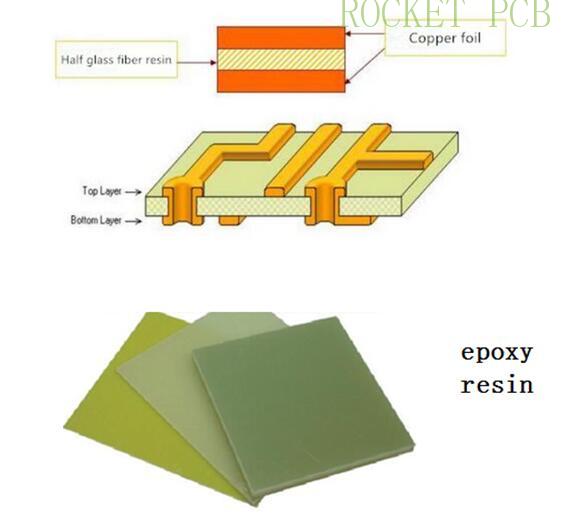
The common PCB material is CCL-FR4.
FR-4 is the code of a fire-resistant material grade, which means that the resin material must be able to extinguish itself after burning. It is not a material name, but a material grade.
FR-4 epoxy glass fiber cloth substrate is a kind of substrate with epoxy resin as adhesive and electronic glass fiber cloth as reinforcement material. Its adhesive sheet and inner core thin copper clad laminate are important substrates for making multilayer printed circuit boards.
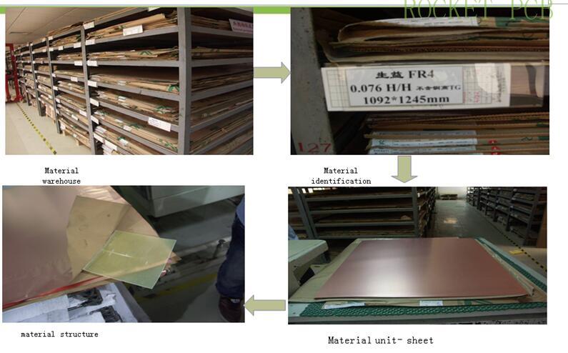
1. Material process
Inspection of incoming materials --- cutting --- grinding edge --- fillet --- cleaning ---baking --- next process
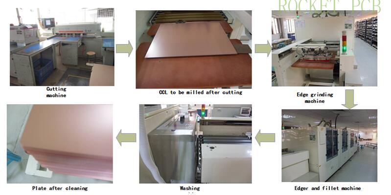
Cutting: according to the size required by engineering MI, the large copper clad laminate is divided into manufacturing unit panel (PNL).
(sheet ---working panel ---set ---piece)

Common materials and specifications:
FR-4 , and the bulk size is 36 "×48", 40 "×48", 42 "×48", 41 "×49", 48 "×72"
Utilization rate of cutting material:
The utilization ratio is the percentage of finished product delivery area and cutting area.Generally, the requirement of double-sided PCB is more than 85%, and that of multilayer board is more than 75%.
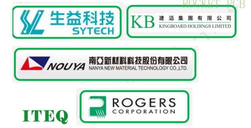
Common PCB material suppliers
2. Drilling
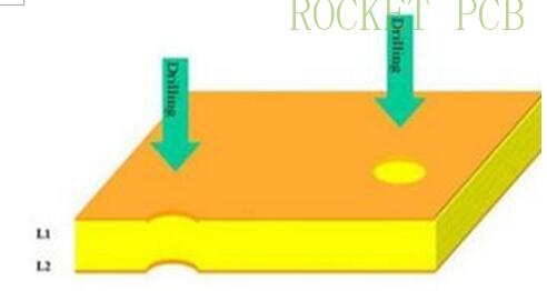
Drilling principle
Use the drill bit on the drilling rig to drill the required holes on the circuit board at high speed and falling speed.

Production process flow:
Drilling positioning hole--- loading board--- input data--- drilling--- head board inspection--- shooting red film--- grinding burr--- next process
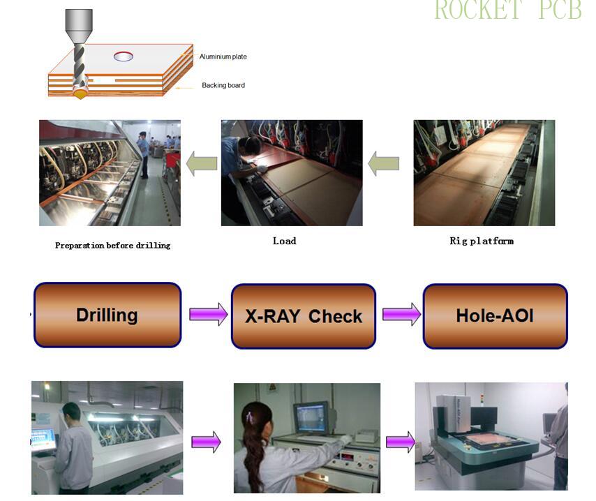
Aluminum sheet : Aluminum sheet plays the role of heat conduction, positioning, reducing the burr of orifice and preventing the scratch of board surface.
Backing board: Mainly a composite board, which protects the rig table during the manufacturing process; prevents export burrs; reduces the temperature of the drill and cleans the slag of the drill
Polishing burr: Due to the different material of the board, there is a burr at the edge of the hole. After drilling, it is necessary to use a manual grinding machine to grind off the burr.
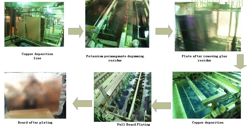
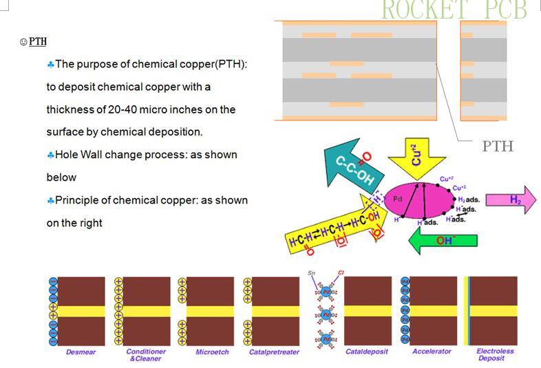
3. Copper deposition-PTH Electroless plating Process
After drilling PCB board, through chemical treatment, deposit (cover) a layer of uniform, heat-resistant impact metal copper in the drilled hole.
The function of copper deposition is as follows
A layer of copper is covered in the drilled hole to realize the circuit connection between PCB layers and realize the plug-in welding function at the customer's site.
Production process flow:
Grinding ---clear up hole--- washing--- micro etching--- washing --- pre leaching --- activation--- washing ---Acceleration--- washing---chemical copper ---washing ---next step
Deburr:
Reasons for the formation of burrs: uncut copper wire and glass cloth at the edge of the hole after drilling. The purpose of deburring: to remove the burrs at the edge of the hole to prevent poor plating.
Important raw materials: abrasive brush
Desmear:
Reasons for the formation of glue slag: the high glass transition temperature (Tg value) caused by drilling, which forms a molten state, which produces glue slag
The purpose of removing glue slag: expose the copper rings to be interconnected in each layer, and another leavening agent can improve the hole wall structure and enhance the adhesion of electroplated copper.
Important raw materials: KMnO4 (glue remover)
Full board plating: A layer of copper is electrodeposited in the hole after copper deposition to realize the reliable interconnection of layer patterns.
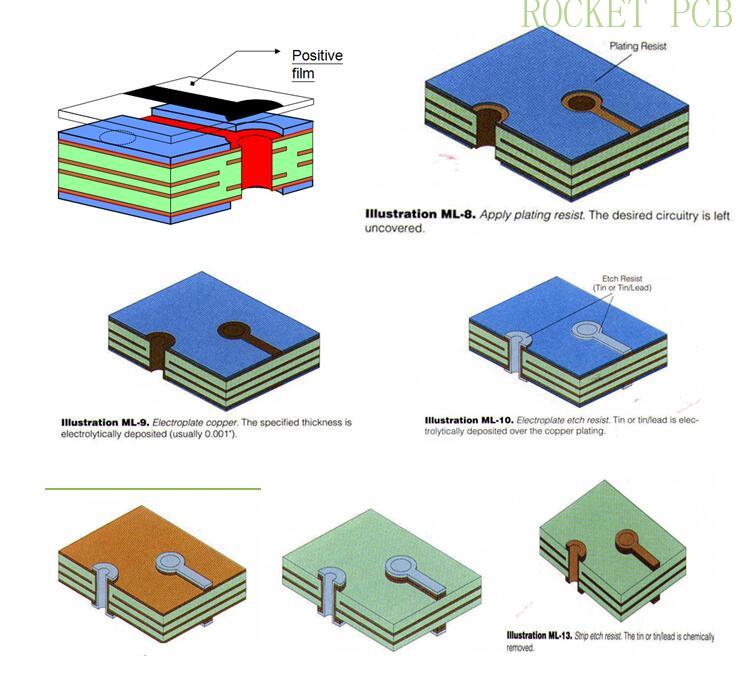
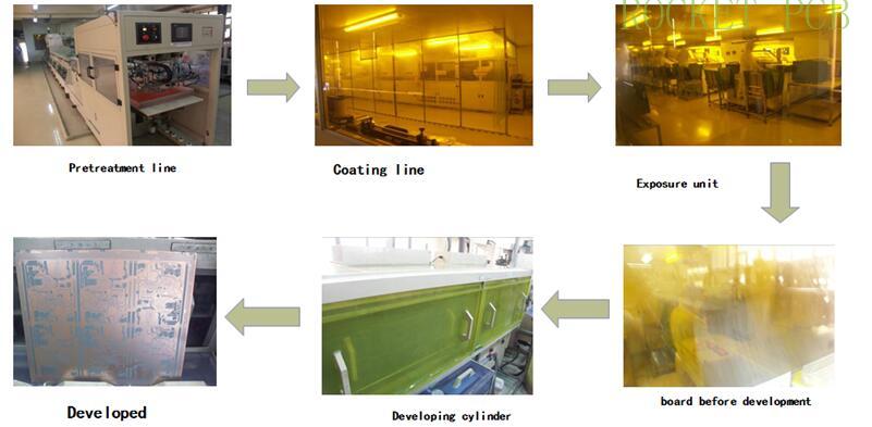
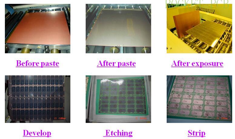
4. Outer pattern process
The pre-processing board is pasted with photosensitive layer (dry film), and aligned with film pattern. Then, the aligned PCB is sent to the exposure machine for exposure, and then the unreacted photosensitive layer is dissolved through the developer, and finally the required circuit pattern is obtained on the copper plate.
Production process flow:
Pre-treatment --- Paste film--- Position--- Exposure ---Development ---Pattern plating(Copper and Tin)---Strip film---Etching---Strip Tin--- QC inspection--- next step

A. Pretreatment (super coarsening)
The finished plate is sent into the equipment to form a copper surface with high roughness under the joint action of spray, temperature, liquid medicine and speed, thus increasing the adhesion between dry film and copper surface.
B. Dry film application
Firstly, the polyethylene protective film is peeled off from the dry film, and then the dry film corrosion inhibitor is pasted on the copper clad laminate under the condition of heating and pressure. The resist layer in the dry film becomes soft after being heated and the fluidity is increased. Then the film is pasted with the help of the pressure of the hot pressing roller and the role of the binder in the resist.
C. Exposure
Under UV irradiation, photoinitiators absorb light energy and decompose into free radicals. The free radicals lead to photopolymerization monomers for cross-linking reaction. After the reaction, stereoscopic macromolecular structure insoluble in weak base is formed.
D. Development
The active group in the unexposed part of the photosensitive film reacts with the weak alkali solution to form a soluble substance to dissolve; the unexposed photosensitive film reacts with the developer and is dissolved, and the exposed film does not react with the weak alkali solution and is retained, so as to obtain the required circuit pattern.
-------------
E Pattern plating( plating copper and Tin)
Electroplating definition:
Electroplating is a process in which the metal or alloy is deposited on the surface of the workpiece by electric current to form a uniform and dense metal layer with good adhesion.
Purpose of electroplating:
Increase the thickness of wire and hole coating, improve the electrical properties and physical and chemical properties of the coating in the hole.
The function of the lead tin plating process is to provide a protective coating to protect the copper wire of the graphic part from being corroded by the etching solution.
F. Etching
A. Principle:
The unprotected copper is dissolved by chemical method, the protected copper is left, and then the protective layer (tin layer) on the circuit layer is removed. Finally, the required circuit pattern is obtained on the bare copper plate.
B. Production process:
Place ---Strip--- Washing--- Etching --- Washing--- Strip Tin--- washing--- Baking --- QC inspection
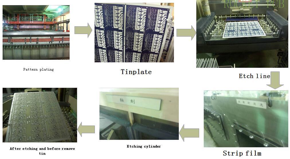

Illustration of outer pattern process
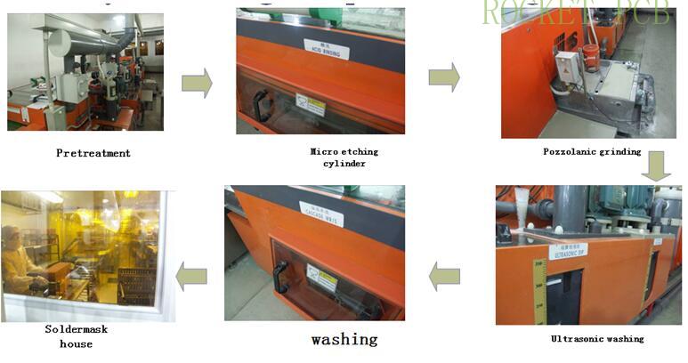
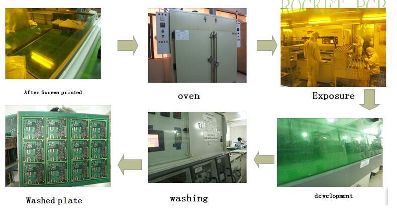
5. Soldermask process
Principle:
After pretreatment, solder mask ink is printed to the board surface through screen. Under certain temperature, time and air volume, the solvent in the ink will evaporate initially. Then, the pad and hole required by the customer will be protected by film graphics for exposure. The ink that does not react with UV light will be dissolved during development, and finally the pad and hole required by the customer can be obtained
Function of soldermask:
1. Beautiful
2. Protection
3. Insulation
4. Anti welding
5. Acid and alkali resistant
Production process:
Grinding board---silk screen solder mask --- pre-baking--- exposure ---Develeping ---PQC inspection--- post-curing--- next process
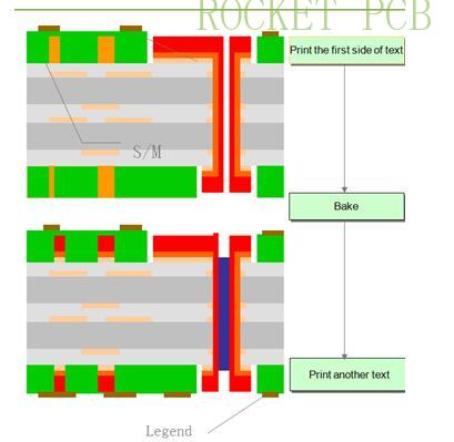
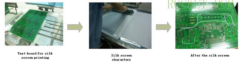
6. Silkscreen process
Principle:
Under a certain force, the character ink required by customers can be printed on the surface of PCB board through a certain number of mesh screen screen, which can provide information for component installation and future maintenance of PCB board
Production process:
Check the lot card to determine whether it is necessary to screen the characters and the character production requirements ---According to the requirements of the lot card, select the character ink --- turn on the oil --- check whether the character net is qualified --- Alter the Date code --- Lock the screen plate on the screen printing machine---- para-position --- Head board printed --- After the first plate is OK, print in batches---collect oil --- clean the screen plate --- Remove the screen plate
Character ink type:
Character ink is thermosetting ink, when it is thermosetting, even with strong acid and alkali are difficult to clean it.
Common defects:
Characters on pad, Character blur, less oil on characters, characters sticking on board, etc.
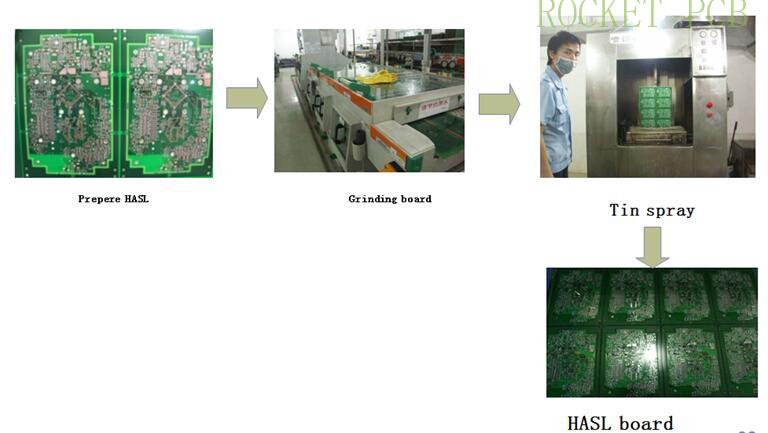
7. Surface treatment
A conventional printed circuit board (PCB) has copper layers on the board. If the copper layer is not protected, it will be oxidized and damaged, which directly affects the subsequent soldering.
There are many different protective layers that can be used, the most common ones are: Hot Air Leveling (HASL), OSP, Plating Nickel & gold, Immersion Nickel Gold (ENIG), Gold Finger, Immersion Silver and immersion Ti etc.
(1) Hot air leveling (HASL): After the board is completely covered with solder, then the high-pressure hot air is used to blow off the excess solder in the surface and the hole, and the solder attached to the pad and the hole wall is leveled; there are lead soldering and lead-free soldering two kinds.
Advantages: low cost, maintain solderability throughout the manufacturing process
(2) Organic coating (OSP): A thin, uniform protective layer is formed on the copper surface of the PCB.
Advantages: Comparable with HASL in cost, good coplanarity, lead-free process
(3) Plating gold: plating nickel and protective gold on copper surface by electroplating.
Advantages: good weldability, flat surface, long storage life, can withstand multiple reflow soldering.
(4) ENIG: Replace the nickel-phosphorus layer on the copper surface through a chemical reaction, and then replace a layer of gold on the nickel layer.
Advantages: good solderability, flat surface, long storage life, can withstand multiple reflow soldering
(5) Gold finger: Nickel and gold are electroplated on the edge copper surface of board by electroplating, because gold plating contains other metals, it's different with (3).
(6) Immersion Silver: Silver is immersed in a 0.1 to 0.6 micron metal layer on the copper layer to protect the copper surface.
Advantages: good weldability, smooth surface, natural replacement of HASL immersion.
(7) Immersion Tin: Tin is immersed in a metal layer of 0.8 to 1.2um on the copper layer to protect the copper surface.
Advantages: good weldability, smooth surface, relatively low cost.
HASL Production process:
Micro etching ---washing--- Apply flux---HASL--- Air bed cooling--- Hot water washing--- Water washing--- Drying--- PQC inspection--- Next process
Comparison of melting points of alloy solders:
The melting point of lead solder is 183 ℃ (Sn63 / Pb37)
The melting point of lead-free solder is 227 ℃ (Sn / Cu / Ni)
ENIG production process

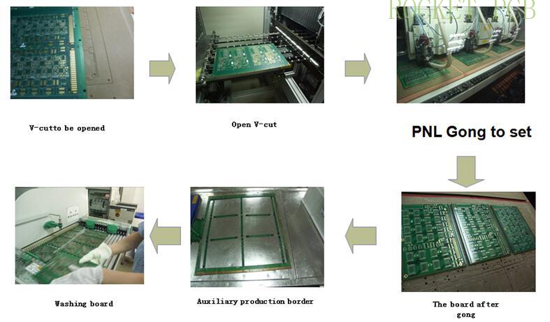
8. Profiling/routing
Principle:
Input the data (Gong route) into the CNC milling machine, and divide the PNL board (Gong board) into the external dimensions required by customers.
Production process:
Drilling positioning holes--- put on the board input data--- Gong--- cleaning finished board--- next process
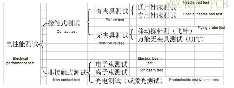
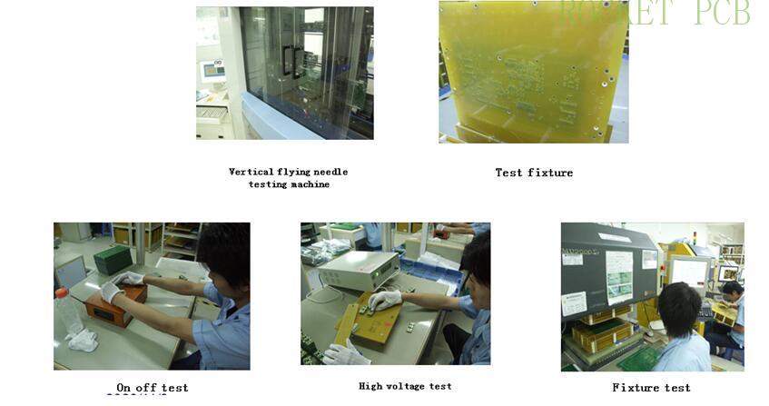
9. Electrical test
The electrical performance test of PCB is usually called "on", "off" test or "on" and "short" circuit test to check whether the network status of the produced PCB board meets the design requirements of the original PCB
Principle:
Connectivity test: apply current to one end of a network to be tested, measure the other end of the network, and judge whether the network (wire) is on or off and the resistance value according to the change value of current
Insulation test: apply voltage to a network (wire) to be tested, and detect whether there is voltage value on other adjacent network, so as to judge whether the network (wire) is insulated.
Test classification:
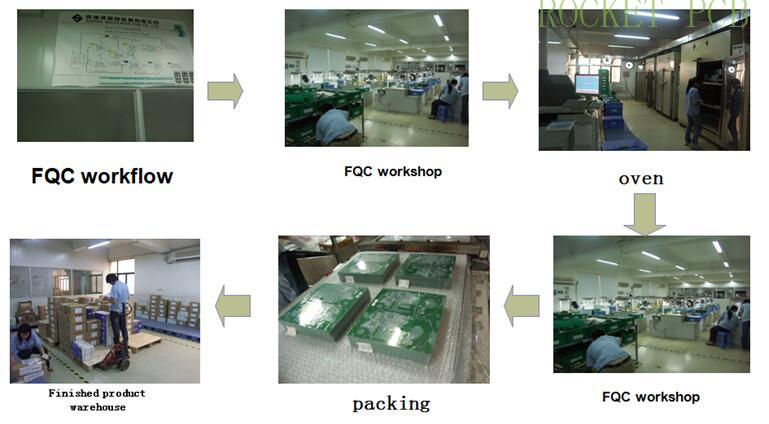
10. Finished product inspection (FQC)
According to the customer's acceptance standard and our company's inspection standard, the appearance of the finished PCB board is inspected, and if there is any defect, it is repaired in time to ensure that it provides customers with excellent quality control.
11. Final inspection / laboratory
Final inspection / laboratory is the final quality check conducted during the manufacturing.
1) The main items of inspection:
1. Outline Dimension
2. Hole to Edge
3. Board Thickness
4. Holes Diameter
5. Line width/space
6. Annular Ring
7. Items in appearance and length etc.
2) The main project of the laboratory
1. Solderability
2. Peel strength
3. Micro Section
4. Thermal Shock
5. Ionic Contamination
6. Moisture and Insulation Resistance
7. Impedance
8. Reliability and other items.
12. Finished product packaging
1. Cutting material
Cutting the material to required size for inner layer and outer layer (working panel).
2, Inner pattern process
The uncoated core board is treated with pre-treatment micro etching and roughening the copper surface, and then the core plate coated with the photosensitive layer is exposed with production film to make the photosensitive layer of the circuit part polymerize and cross-linked. After weak alkali development, the unreacted photosensitive layer is dissolved to expose the copper surface, and then exposed by acid etching, Part of the copper is etched away, leaving the copper in the area covered by the photosensitive layer and forming a circuit pattern.This process is the process of film graphics transferring to core board graphics, also known as graphics transfer.
Production process flow:
Pretreatment -Press dry film (wet film)- Exposure - Development--- Etching - stripping film - QC inspection (through AOI) - next process
Pretreatment (chemical cleaning line):
3% - 5% acid solution is used to remove the oxide layer on the copper surface and the protective layer on the original copper substrate to prevent copper from being oxidized, and then micro etching treatment is carried out to obtain fully roughened copper surface and increase the adhesion property between dry film and copper surface.
Apply wet film or press dry film:
Firstly, the polyethylene protective film is peeled off from the dry film, and then the dry film corrosion inhibitor is pasted on the copper clad laminate under the condition of heating and pressure. The resist layer in the dry film becomes soft after being heated and the fluidity is increased. Then the film is pasted with the help of the pressure of the hot pressing roller and the role of the binder in the resist.
Dry film exposure principle:
Under UV irradiation, photoinitiators absorb light energy and decompose into free radicals. The free radicals lead to photopolymerization monomers for cross-linking reaction. After the reaction, stereoscopic macromolecular structure insoluble in weak base is formed.
Development principle, etching and stripping:
The active group in the unexposed part of the photosensitive film reacts with the weak alkali solution to form a soluble substance to dissolve; the unexposed photosensitive film reacts with the developer and is dissolved, and the exposed film does not react with the weak alkali solution and is retained, so as to obtain the required circuit pattern.
Etching
Stripping film
The change of Board on line
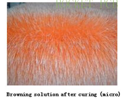
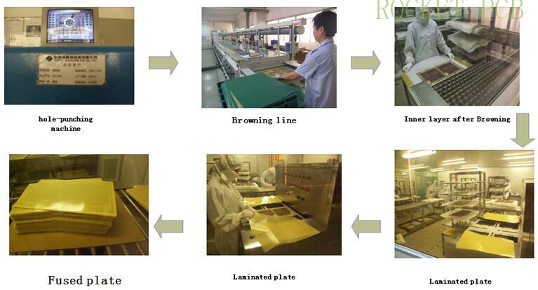
3. Browning:
The purpose of browning is to increase the surface roughness of copper foil and increase the contact area with resin, which is conducive to the full diffusion and filling of resin.
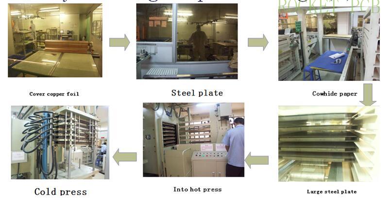
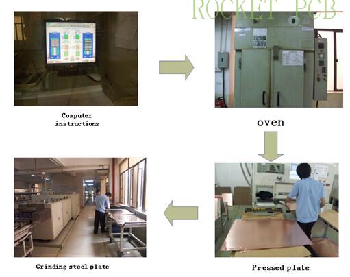
4. Lamination
According to the MI requirements, the inner core board and PP sheet are stacked together and fixed. According to the process parameters, the inner core board and PP sheet are pressed together to form a complete Multilayer PCB under certain temperature, pressure and time conditions.
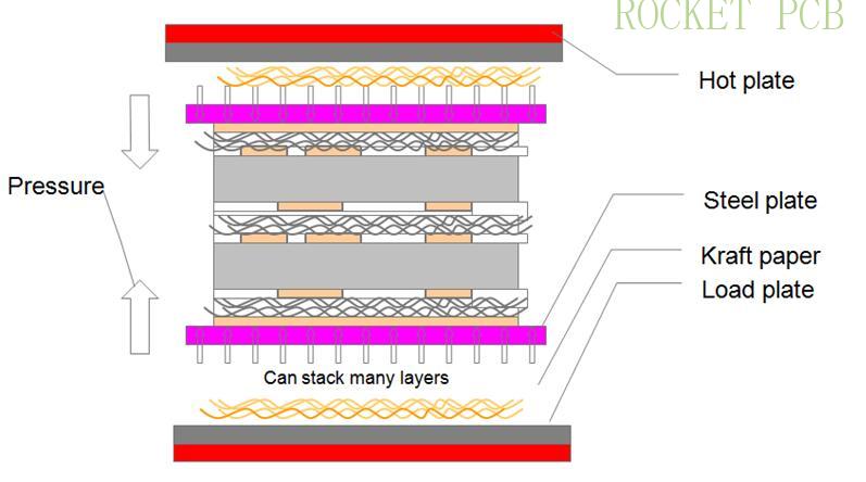
Production process flow:
Browned ---Riveting---Pre stack ---Stack --- hot pressing --- cold pressing--- dismantle--- X-ray---drilling --- Gong edge--- next step
The next drilling, PTH process , outer pattern process and the following processes of multilayer PCB are the same with that of two layers board.
That is,
5. Drilling
6. Electroless copper
7. Full board plating
8. Outer pattern process
9. Soldermask
10. Silkscreen
11. Surface treatment
12. Profiling
13. FQC
14.Package


