Classification of ceramic PCB
1. Classification by ceramic material
Al2O3
Alumina substrate is the most commonly used substrate material in the electronic industry, because in terms of mechanical, thermal, and electrical properties, compared with most other oxide ceramics, its strength and chemical stability are high, and the source of raw materials is rich, which is suitable for various technical manufacturing and different shapes.
BeO
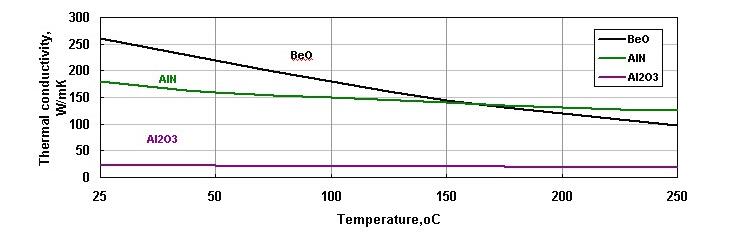
It has higher thermal conductivity than aluminum, so it can be used in occasions where high thermal conductivity is needed. However, when the temperature exceeds 300 ℃, it decreases rapidly. The most important reason is that its toxicity limits its development.
AlN
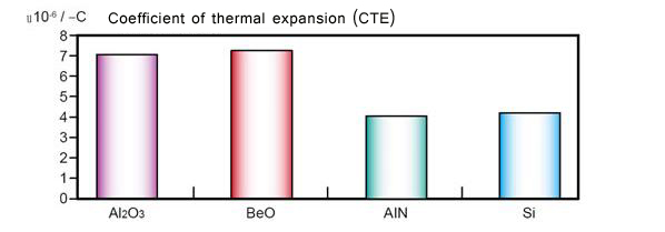
AlN has two very important properties to note: one is high thermal conductivity, the other is the expansion coefficient matching with Si. The disadvantage is that even if there is a very thin oxide layer on the surface, the thermal conductivity will be affected. Only by strictly controlling the material and process, can the AlN substrate with good consistency be produced. However, with the improvement of the economy and technology, this bottleneck will eventually disappear.
From the above reasons, we can know that alumina ceramics(Al2O3) are still in a leading position in microelectronics, power electronics, Hybrid Microelectronics, power modules and other fields due to their superior comprehensive properties.
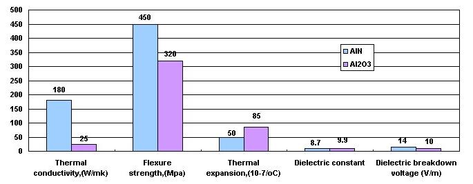
Comparison of aluminum nitride (AlN) and aluminum oxide(Al2O3) characteristics
2. According to the ceramic PCB manufacturing process
At present, there are five kinds of ceramic heat dissipation substrates: HTCC, LTCC, DBC, DPC, and Lam. HTCC / LTCC belongs to the sintering process, and the cost will be higher.
HTCC (High-Temperature Co-fired Ceramic)
HTCC is also known as high-temperature co-fired multilayer ceramics. The manufacturing process of HTCC is very similar to that of LTCC. The main difference is that the ceramic powder of HTCC is not made of glass. Therefore, HTCC must be dried and hardened to form an embryo at 1300 ~ 1600 ℃, and then the through-holes are drilled, and the holes and printed circuits are filled with screen printing technology. The main materials are tungsten, molybdenum, and manganese with high melting points but poor,conductivityFinally, it is sintered in layers.
LTCC (Low-Temperature Co-fired Ceramic)
LTCC-It is also called low-temperature co-fired multilayer ceramic substrate. In this technology, inorganic aluminum oxide powder and about 30% ~ 50% glass material are added with an organic binder to make it evenly mixed into a mud-like slurry. Then, the slurry is scraped into flakes by a scraper, and then the flake slurry is formed into thin pieces by a drying process. Then, through-holes are drilled according to the design of each layer as the signal of each layer. The inner circuit of LTCC uses screen-printing technology to fill holes and paint lines on the green embryo respectively. The inner and outer electrodes can use silver, copper, gold, and other metals respectively. Finally, each layer is stacked and placed in a sintering furnace at 850 ~ 900 ℃ for sintering and molding.
DBC (Direct Bonded Copper)
Direct copper deposition technology is to uses the oxygen-containing eutectic liquid of copper to directly coat copper on ceramics. Its basic principle is to introduce an appropriate amount of oxygen between copper and ceramics before or during the bonding process. In the range of 1065 ℃ ~ 1083 ℃, copper and oxygen form Cu-O eutectic liquid. DBC technology uses the eutectic liquid to produce a chemical reaction with ceramic substrateCualo2 or cual2o4 phase, on the other hand, infiltrate copper foil to realize the combination of the ceramic substrate and copper plate.
DPC (Direct Plated copper)
At present, the traditional LC and DBC technology is gradually replaced by DPC, and the laser technology is more in line with the high-density interconnection and fine development of printed circuit boards. The results show that the ceramic circuit board with laser drilling technology has a high bonding force between ceramic and metal, no shedding and bubbling, and can grow together. The surface roughness is high, the roughness is between 0.1μm ~ 0.3 μm and the laser hole diameter is 0. 15 mm-0. 5 mm, or even 0.6 mm.
DBC is the combination of Al2O3 and Cu plate by high-temperature heating. The technical bottleneck of DBC is that it is difficult to solve the problem of micropores between Al2O3 and Cu plate, which makes the mass production energy and yield of the product face great challenges. However, DPC technology uses direct copper plating technology to deposit Cu on the Al2O3 substrate. Its process combines materials and film technology, and its products are most commonly used in recent years ceramic heat dissipation substrate. However, the requirement of material control and process technology integration ability is high, which makes the technical threshold of entering the DPC industry and stable production relatively high.
Lam technology
Lam technology is also called laser rapid activation Metallization Technology.
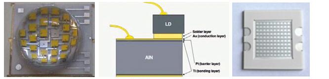
Ceramic substrate-our laser rapid activation metallization (LAM) is at the leading level in the global ceramic PCB industry and can be quickly customized to meet customer needs. The ceramic-based substrate has good thermal and electrical properties. It is an excellent material for power LED packaging, violet light, and ultraviolet. It is especially suitable for the packaging structures of MCM and cob. It can also be used as the heat dissipation circuit substrate of other high-power semiconductor modules, high current switch, relay and antenna of communication industry filter, solar inverter, etc.
The superiority of ceramic substrate PCB
The thermal expansion coefficient of the ceramic substrate is close to that of the silicon chip, which can save the transition layer Mo sheet, save labor, material, and cost;
Reduce welding layer, thermal resistance, cavity and improve yield;
Only 10. 0% of the printed circuit board with the same line width of 0. 3mm;
Excellent thermal conductivity makes the package of the chip very compact, which greatly improves the power density and improves the reliability of the system and device;
Ultra-thin (0. 25 mm) ceramic substrate can replace BeO without environmental toxicity;
The temperature rise is about 17 ℃ when 100A current continuously passes through a copper body with a width of 1 mm and a thickness of 0. 3 mm; a current of 100 continuously passes through a copper body with a width of 2 mm and a thickness of 0. 3 mm, and the temperature rise is only about 5 ℃;
The thermal resistance of 10 × 10 mm ceramic substrate is low. The thermal resistance of 0. 63 mm thick ceramic substrate is 0. 31 K / W, that of 0. 38 mm thickness ceramic substrate is 0. 19 K / W, and that of 0.25 mm thickness ceramic substrate is 0. 14 K / W.
High insulation and withstand voltage ensure personal safety and equipment protection ability.
New packaging and assembly methods can be realized to make the product highly integrated and reduce the volume
PS: Comparison of thermal properties (conductivity):
Glass fiber substrate (traditional PCB): 0. 5w/mk
Aluminum substrate: 1 ~ 2. 2w/mk,
Ceramic substrate: [alumina] 24 ~ 170 [aluminum nitride] W / MK
Material thermal conductivity (unit: w / MK):
Resin: 0. 5
Alumina: 20-40
Silicon carbide: 160
Aluminum: 170
Aluminum nitride: 220
Copper: 380
Diamond: 600
High thermal conductivity ceramic circuit has the advantages of high thermal conductivity: 25W / m. k, high-voltage resistance: above 12kV, high-temperature resistance: - 55-500 degrees, very small high-frequency dielectric loss, repeated manual soldering without desoldering and delamination, general size: 100 * 160mm.
Double sided copper clad circuit, thickness: 0.25/0.38/0.635/0.8/1.0 mm + 0.2 / 0.3 double-sided copper clad circuit, can be plated with gold/nickel. RoHS compliant
Application of ceramic substrate
High power semiconductor module; semiconductor cooler, electronic heater; power control circuit, power mixing circuit.
Intelligent power module, high-frequency switching power supply, solid-state relay.
Automotive electronics, aerospace, and military electronic components.
Solar panel module; telecommunication special exchange, receiving system; laser and other industrial electronics.
Comparison of plastics and ceramics
So far, plastics, especially epoxy resin, have dominated the electronic market due to their better economy. However, many special fields such as high temperature, mismatch of linear expansion coefficient, airtightness, stability, and mechanical properties are obviously not suitable. Even if a large amount of organic bromide is added to the epoxy resin, it will not help.
Compared with plastic materials, ceramic materials have high resistance, outstanding high-frequency characteristics, high thermal conductivity, good chemical stability, thermal stability, and high melting point. In the design and manufacture of PCB circuits, these properties are very needed. Therefore, ceramics are widely used as substrate materials for different thick films, thin films, and circuits, as insulators, as heat conduction paths in circuits with strict thermal performance requirements, and for manufacturing various electronic components.
Manufacture of the ceramic substrate
It is very difficult to produce high-purity ceramic substrate. Most ceramics have high melting points and hardness, which limits the possibility of ceramic machining. Therefore, glass with a low melting point is often doped in the ceramic substrate for fusing or bonding, so that the final product is easy to be machined. The preparation process of Al2O3, BeO, and AlN substrates is very similar. The matrix materials are ground into a powder with a diameter of about a few microns, and mixed with different glass fluxes and adhesives (including MgO and Cao of the powder). In addition, some organic adhesives and different plasticizers are added to the mixture to prevent agglomeration, so that the composition is uniform, and the raw ceramic chips are formed, and finally sintered at high temperature.
Relationship between PCB, ceramic substrate and LTCC
LTCC means low-temperature CO firing of ceramics. Since the maximum sintering temperature of silver is 920 ℃, in order to lay silver wires on the ceramics, low-temperature CO firing is carried out. If silver lines are printed on the inside and on the surface of the ceramics, and they are burned together with the ceramics, that is, the so-called ceramic substrate. The ceramic plates with two functions of heat dissipation and lead wires on the top and bottom of LED lamps are ceramic substrates. Of course, there are also those that are not used as substrates. At present, circuit boards are mostly composed of organic materials. Nowadays, in order to achieve greater integration, many capacitors, resistors, and inductors are expected to be integrated into PCB boards. Most of these are ceramic raw materials and need high-temperature sintering. We think of ceramic plates with good insulation performance and high-temperature sintering, and the ceramic dielectric constant is adjustable
Difference between the ceramic substrate and common PCB
At present, the FR-4 circuit board is the most widely used in the market, but the defects of the FR-4 circuit board are irreversible. FR-4 copper clad laminate has the advantages of no insulation layer, mass production, fast molding, and low price, but the defects are also obvious,
1. Thickness out of tolerance
2. Substrate delamination
3. White spot on the substrate
4. Exposed pattern on the substrate
5. Impurity and black spot on the substrate
6. Copper foil wrinkle
7. Glue spot
8. Pit
9. Pinhole
10. Copper foil oxidation
11. Copper foil bright spot
12. Light concave
13. Steel grain: copper clad laminate with steel plate pattern will cause wavy phenomenon on copper foil surface for fine line PCB production
14. Uneven filling problem
15. Insufficient curing of the substrate is obvious, and edge burr is more
16. Common defects of prepreg
17. CAF (substrate resistance to ion migration)
Advantages of the ceramic circuit board
1. High resistance
2. Outstanding high-frequency characteristic
3. High thermal conductivity
4. Good chemical stability, shock resistance, heat resistance, withstand voltage, internal circuit, mark point, etc. are better than the general circuit board.
5. It is accurate in printing, mounting, and welding
Disadvantages of the ceramic circuit board
1. Fragile: This is the main drawback, only a small area circuit board can be made at present.
2. High price: there are more and more requirements for electronic products. The ceramic circuit board can only meet the requirements of some high-end products, and low-end products will not be used at all.
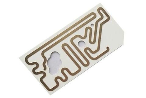
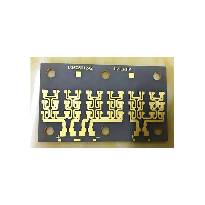
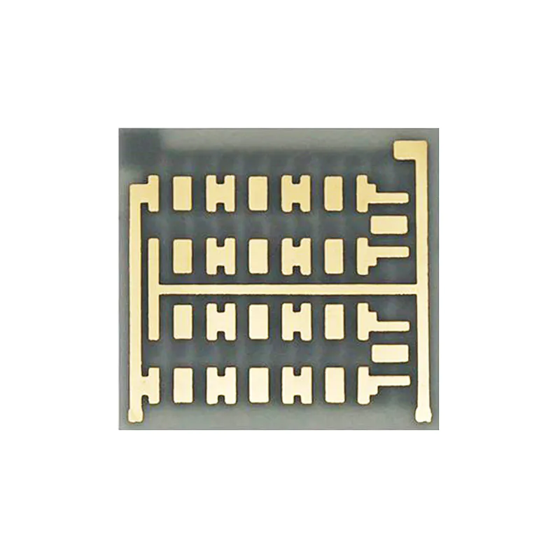
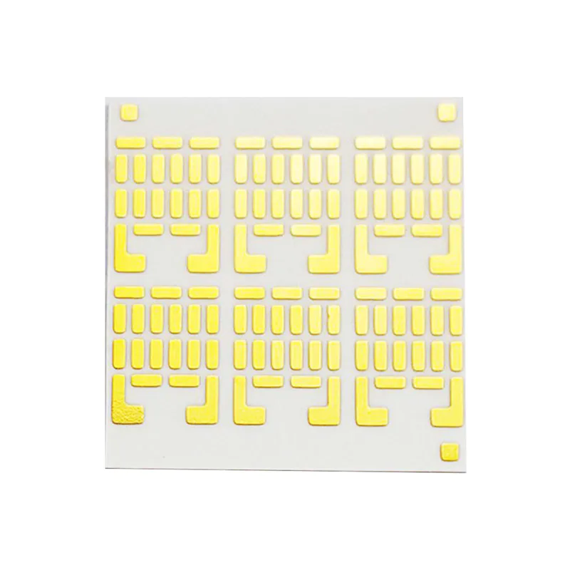
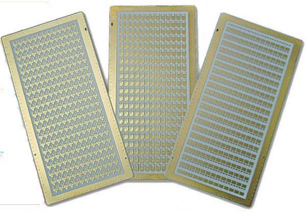
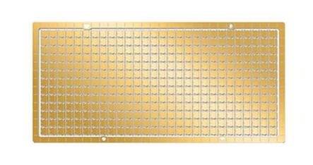
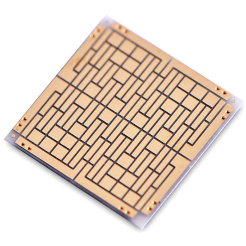
Ceramic PCB from us
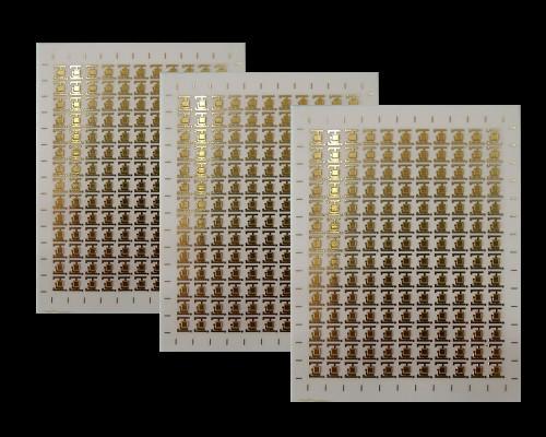
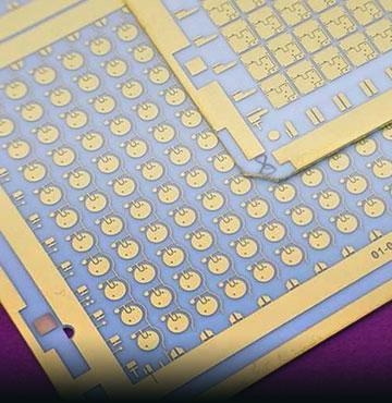
As for the ceramic substrate, the alumina (Al2O3) ceramic circuit board and aluminum nitride (AlN) ceramic circuit board are relatively mature. Many companies can make 3535, 5050, 7070 and so on.
Rocket PCB can be customized by customers. No matter what specification it is, it can be made. However, the distance between lines should be greater than 20 microns, and full-automatic production should be adopted.
This kind of product mainly exists in products with high heat dissipation requirements, such as general aerospace, automotive electronics, lighting, high-power electronic components, so as to maximize product performance.
The ceramic PCB industry is estimated to have a market value of 6 billion US dollars in the lighting market and beat most sunrise industries with an annual growth rate of 7%. It has become a new high-tech enterprise in the industry and has been widely used in subway, rail transit, GBT new energy vehicles, etc.
In today's broad market prospects, Rocket PCB focuses on the production of world-class quality ceramic PCB, enhance brand influence, focus on scientific research and development, and high-tech application, to provide you with timely, intimate, and cost-effective PCB services.