


Teach you how to make simple PCB at home- Photosensitive method
Printed circuit board (PCB) is an important electronic component. Because it is made by electronic printing, it is called "printed circuit board".
Electronic enthusiasts of PCB production methods are mainly heat transfer printing, photosensitive wet film method, photosensitive dry film method. I personally think that the photosensitive wet film method is better to use. There are always bubbles in the dry film method.
Photosensitive method to make PCB is anti etching photosensitive ink on the surface of the copper clad laminate need to retain the part of the protection.The main component of anti etching photosensitive blue paint is negative photoresist, and the part of negative photoresist will decompose if it is not irradiated. The baffle is printed on sulfuric acid paper or film by printer. The baffle is just a negative film of PCB layer in manufacturing. Before the photoresist on the PCB is exposed to UV light, the shield covering it can prevent some areas of photoresist from being exposed (assuming positive photoresist is used). These areas that are covered with photoresist will become wiring.
Raw materials required:
CCL
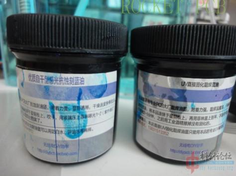
Anti etching photosensitive blue paint
UV direct curing solder resist blue paint
Tools:
Ultraviolet tube
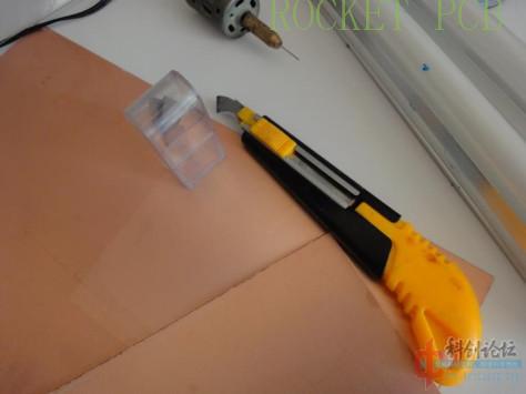
Tools for cutting copper clad laminate (hook, knife and saw blade)
Developer
Etchant
Release agent
Industrial ethanol
Brush
Etching groove
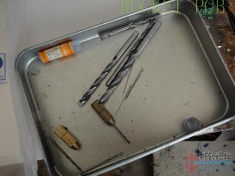
Electric drill
All kinds of drills, 0.5mm 0.7mm 0.8mm 1mm 1.5mm 3mm
One computer (including keyboard, mouse, operating system and printer)
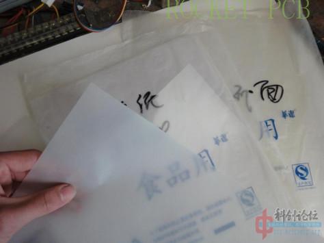
Sulfuric acid paper, film
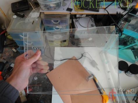
Plywood (6 mm plexiglass board) in fact, two transparent boards are OK
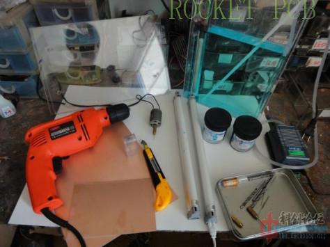
Tool display
Developer, etching agent and release agent:
Developer:
sodium bicarbonate
The dissolution ratio is 1:70 (20g corresponds to 1.5L water)
The developing temperature is between 30 ℃ and 40 ℃
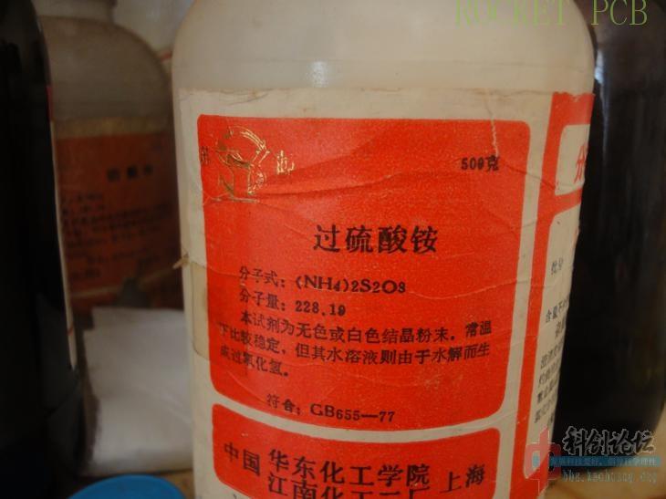
Etchant:
Ammonium persulfate
The dissolution ratio is 1:8 (190g corresponds to 1.5L water)
The etching temperature is between 40 ℃ and 60 ℃
Release agent:
sodium hydroxide
The dissolution ratio is 1:80 (20g corresponds to 1.5L water)
The etching temperature is between 40 ℃ and 50 ℃
General steps
1, Design PCB
2, PCB Plot (Copper Cladding And Solder Mask)
3, Resist Etching Layer Exposure
4, Anti Etching Layer Development
5, Etching
6, Solder Mask Exposure
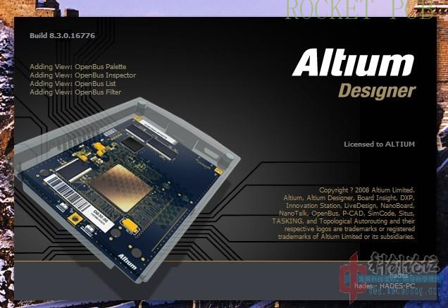
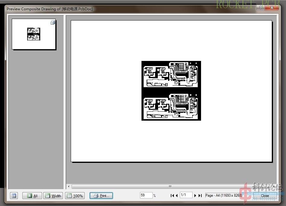
The PCB drawing software I used is DXP AD10. The main interface is shown in the figure below.
First of all, make sure there are two clear layout drawings, one for etching and the other for solder mask.
Both etch and solder mask are negative because most of the resist resist paints are negative photoresists. That is, the irradiated part is left to be removed. So this needs to be set in AD10.
Open ‘file’and select page settings. In the page design interface, select the zoom ratio. Select the custom scale, as shown in the figure below
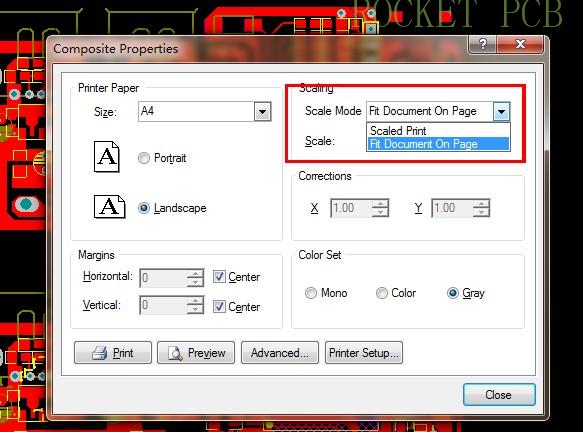
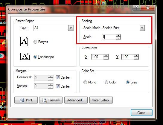
And change the scale to 1, as shown in the following figure.
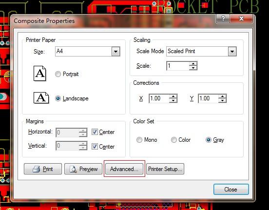
After changing the scale, enter advanced options, as shown below.
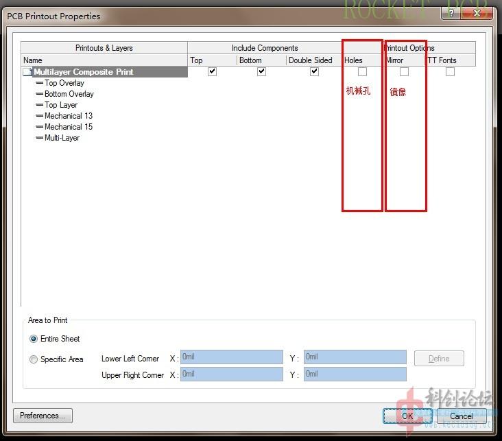
In the advanced options, you can select whether the output image is mirrored and whether the mechanical holes are displayed.
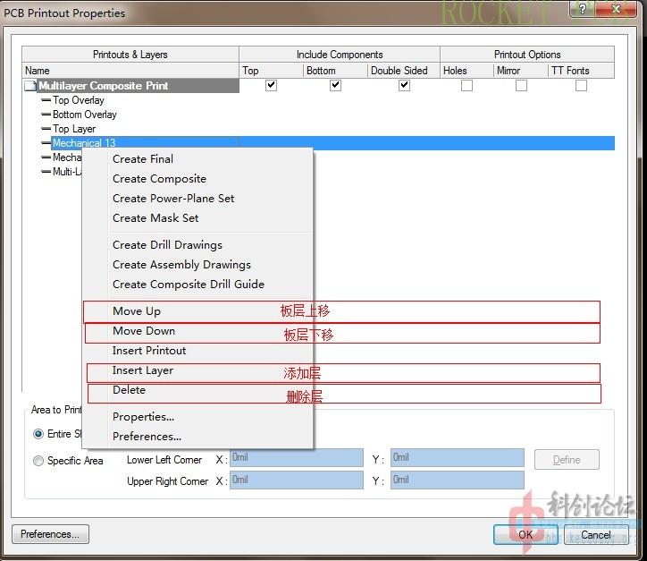
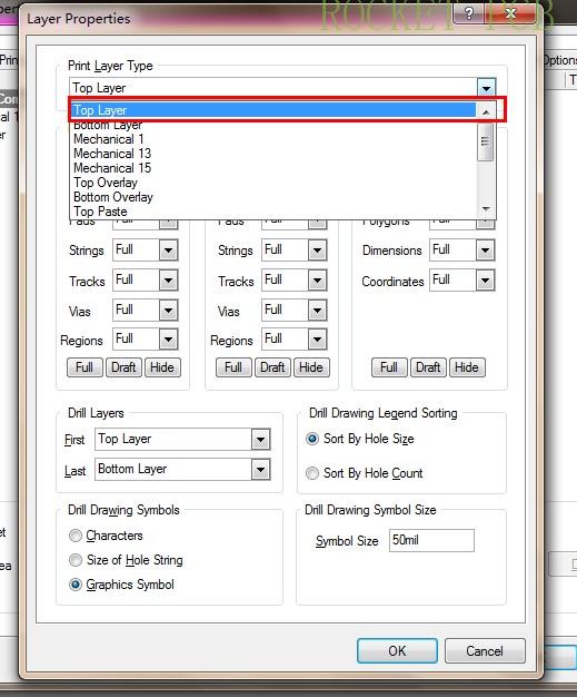
Select the slab layer and right-click to display the following options.
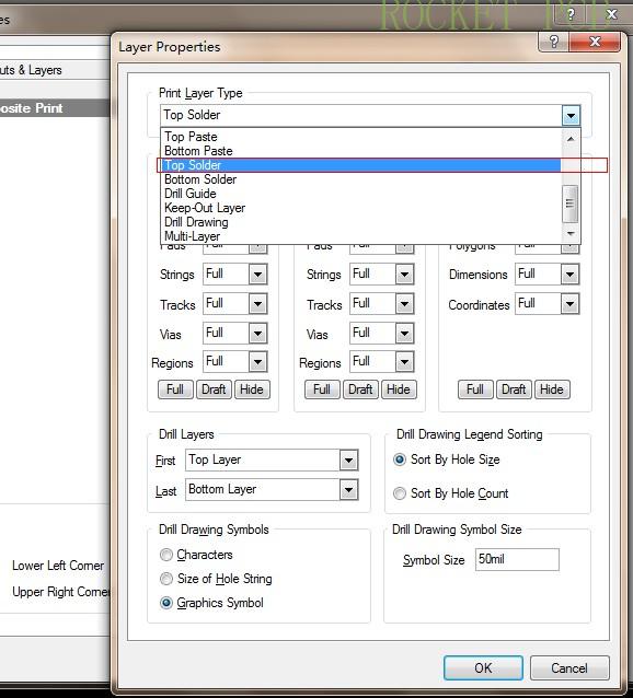
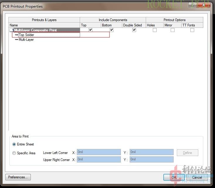
First, the output diagram of solder mask is made. The UV curing solder mask is cured by the irradiated part, that is to say, the part except the pad part is left blank, and the pad part is black to block ultraviolet radiation. All layers except the bottom layer are deleted as follows
Then add the solder mask
As shown in the figure below, do not select the mechanical hole and mirror options
Then click Print Preview, the output diagram is as follows
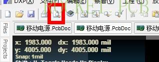
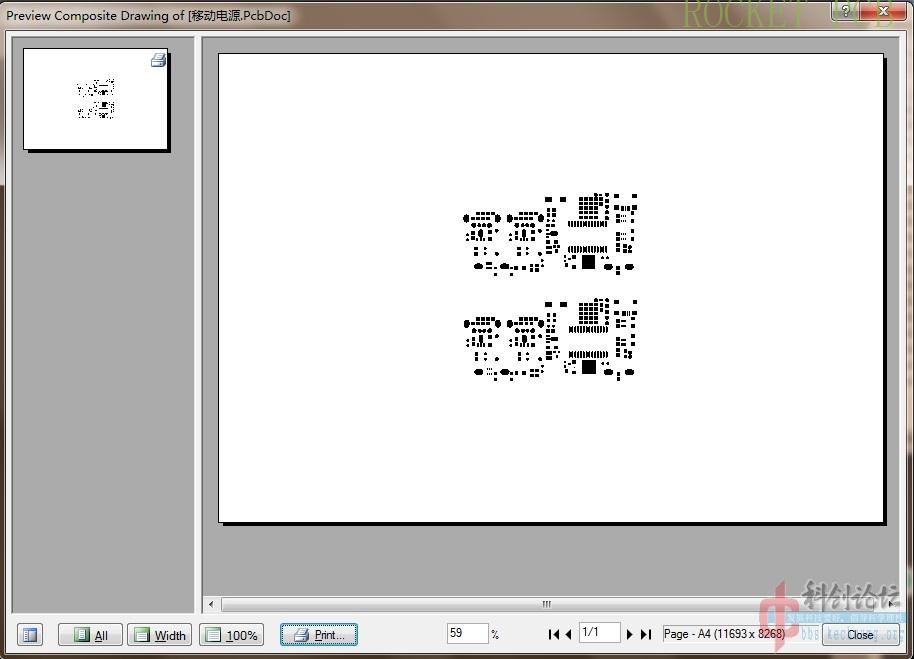


If the output is shown in the figure above, you have successfully set the output configuration
If it’s not the picture above, you need to go over the tutorial carefully
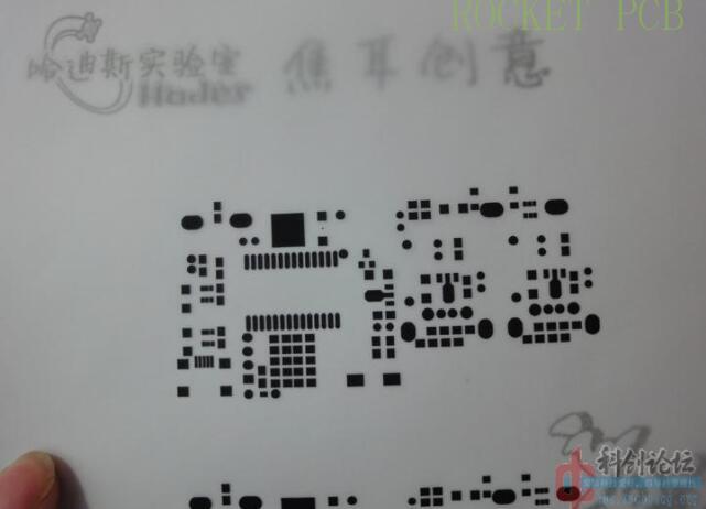
Then the solder mask image is printed on sulfuric acid paper or film.
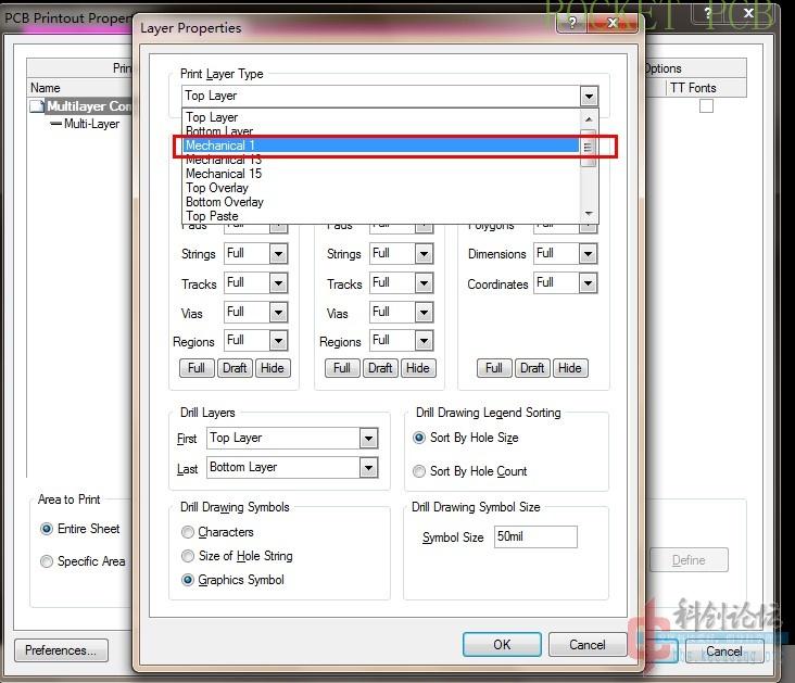
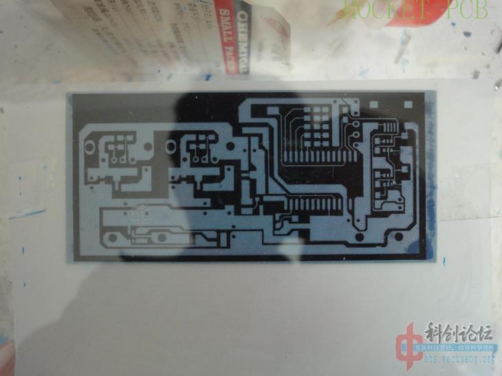
Then there is the anti etching layer. The etching layer requires the output of negative film, and the place of copper coating needs to be left blank
First, delete the unwanted layers
At the bottom of DXP, there is a sheet layer tab. Select mechanical layer 1

Then use the fill tool to cover the board as shown in the figure below
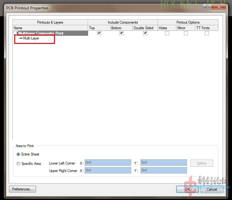
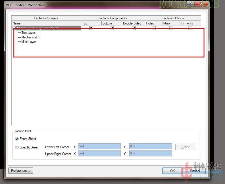
Then the top layer and mechanical layer 1 are added in the interface of the plate layer

After adding, the following layers should be arranged in the following order
The oil can be put into the small sprayer. When I use it, I spray it on the copper clad laminate one by one. That’s how I got it. It works very well.
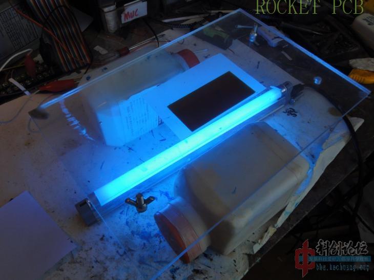
Ultraviolet lamp with 365nm exposure can be dedicated (white or black tube), do not use the transparent tube disinfected by the hospital, the output spectral wavelength range falls outside the sensitive range of photosensitive oil, and can not be exposed normally.
For example, the distance between the exposure time and the exposure time of the lamp is about 10 cm, and the distance between the exposure time and the power of the lamp board is about 10 cm.
Don’t use negative to export, save PDF with virtual printer, then you can go to print shop to print.
Click Print Preview
The copper clad image is then printed on sulfuric acid paper or film.
So you get two boards.

The preliminary work is thus completed~~~
The second big step
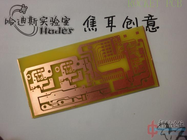
First cut the copper clad laminate according to the required size
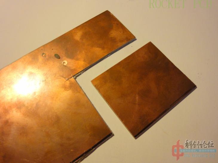
It is suggested to cut from the copper coating surface. After the depth reaches half of the whole plate layer, clear traces can be seen from the reverse side. According to the trace, cut from the back side for several times, and then break it hard to get a complete copper clad laminate~~
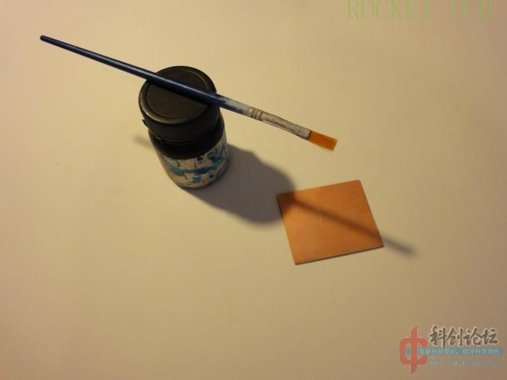
It doesn’t take much skill to apply photosensitive blue paint. If you don’t have a spray pot, you can apply it evenly with a soft brush. If it’s too thick, it’s not good to apply it. It’s recommended to apply it after diluting, and the coating should not be too thick or too thin ~ ~ it’s better that the copper coating can’t be seen just yet~~
Air dryer~~
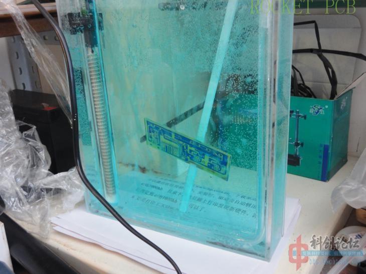
Waiting for exposure
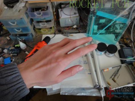
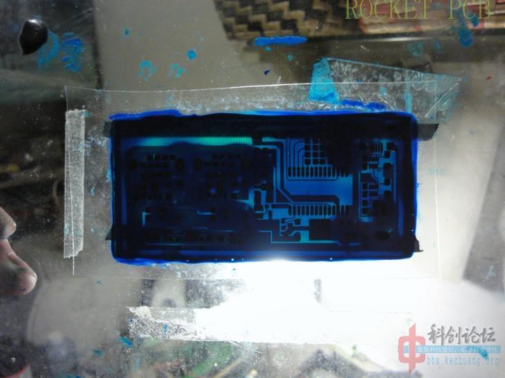
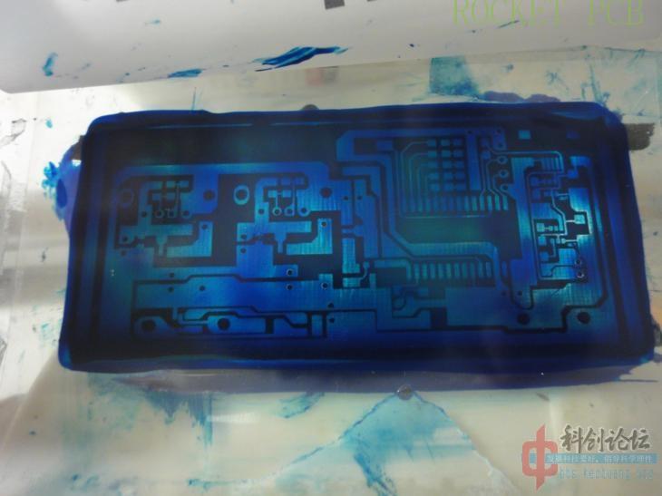
Use a transparent board to align the copper clad laminate with the previous figure and press the two plates tightly with screws

Then exposure, according to different blue oil and UV light tube, the exposure time is slightly different, I am about 4 minutes 15 seconds exposure.
Developer sodium bicarbonate, configuration ratio is 1:70, 20g to 1.5L of water, the temperature maintained at about 30 degrees is better ~ ~ concentration, temperature is too high or too low are not good ~ ~ 30, 40 degrees is the best~~
When developing, pay attention to shake the developer
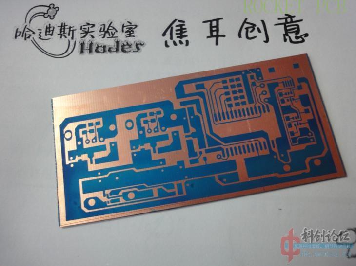
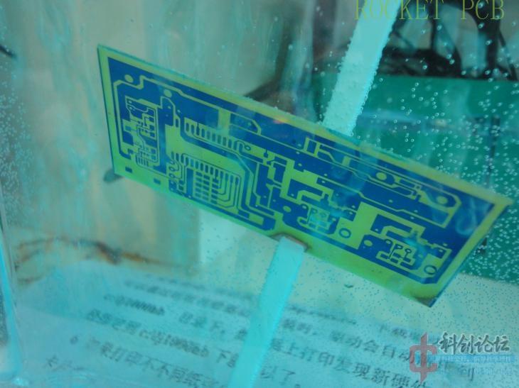
After development, it is as follows
Then etch
The ratio of ammonium persulfate in etchant position is 1:8 190g, corresponding to 1.5 L water, the etching temperature should be controlled between 40 ℃ and 60 ℃
Etch grooves are used
Etching has no other requirements except concentration and temperature requirements.
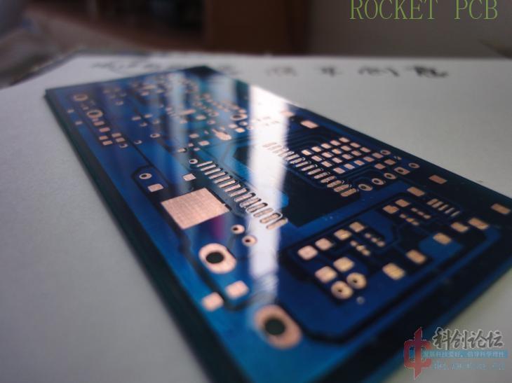
After etching, it is as follows.
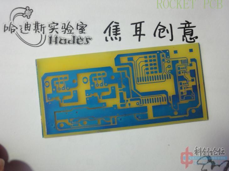
Use release agent to remove the blue paint on the copper surface ~ ~ in fact, sandpaper can be used to grind it off directly~
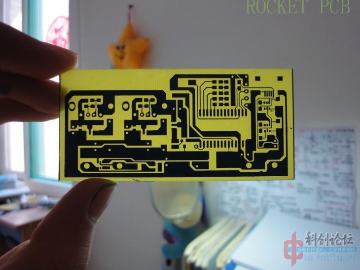
So the second step is done~~
About the production of solder mask, we must want to ask how to make it so smooth.
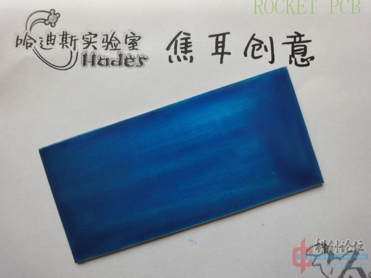
In fact, the solder mask is painted on the copper clad laminate, and then covered with a film. The solder mask made in this way is extremely smooth ~ ~ and then the bubbles are driven out from the middle by various methods. After finishing, it is as follows
Generally, I fix the copper clad laminate on the bottom plate, and then fix it on the bottom plate after aligning the drawing
And then exposed.
Different UV solder blue oil and UV lamp, the exposure time is slightly different, I am about 8 minutes exposure
Finally, the unexposed parts were wiped off with ethanol~~
It’s done!


