


improve your pcb design with these pcb layout tips
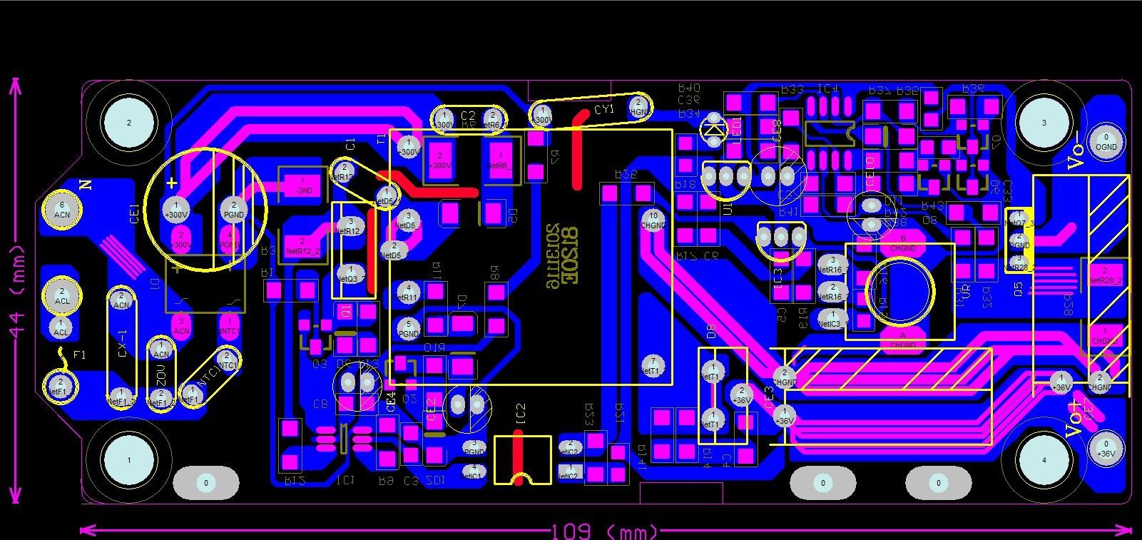
In the design, layout is an important link. The result of layout will directly affect the effect of wiring, so it can be considered that reasonable layout is the first step of PCB design success.
There are two ways of layout, one is interactive layout, and the other is automatic layout. Generally, on the basis of automatic layout, interactive layout is used to adjust the layout. In the layout, the gate circuit can be redistributed according to the route, and the two gates can be exchanged to make it the best layout for easy wiring. After the layout is completed, the design documents and related information can also be returned and labeled on the schematic diagram, so that the relevant information in the PCB board can be consistent with the schematic diagram, so as to synchronize the future archiving and design modification, and update the relevant information of the simulation, so that the electrical performance and function of the circuit can be verified at the board level.
Consider overall beauty
Whether a product succeeds or not, first, we should pay attention to the internal quality, second, we should take into account the overall beauty. Only when both are perfect, can we think that the product is successful.
On a PCB board, the layout of components should be balanced, compact and orderly, cannot be top-heavy.
Layout Inspection
1. Does the PCB size correspond to the drawing size? Can it meet the requirements of PCB manufacturing process? Are there any positioning marks?
2. Are there any conflicts between two-dimensional and three-dimensional components?
3. Are the components arranged in a compact and orderly manner? Is it all finished?
4. Can components that need to be replaced frequently be replaced easily? Is it convenient for plug-in board to insert equipment?
5. Is there an appropriate distance between the thermal element and the heating element?
6. Is it convenient to adjust the adjustable components?
7. Are radiators installed where heat dissipation is required? Is the air flowing smoothly?
8. Is the signal flow smooth and the interconnection shortest?
9. Are plugs and sockets contradictory to mechanical design?
10. Has the problem of line interference been considered?
Layout Principles of Ordinary Components
Arrange the position of each circuit unit according to the circuit flow, make the layout convenient for signal flow, and make the signal as consistent as possible.
On the premise of satisfying the mechanical structure at first, in a given plane space, the basic principle of layout is to arrange the position of each circuit unit according to the circuit flow. In fact, this article also explains how to lay out the main components.
Centering on the core components of each functional circuit, the layout is carried out around it. Components should be evenly, neatly and compactly arranged on PCB. Leads and connections between components should be minimized and shortened.
Layout Principles of Special Components
As far as possible, the wires between high-frequency components should be shortened, and their distribution parameters and electromagnetic interference with each other should be reduced. The components that are susceptible to interference should not be too close to each other, and the input and output components should be as far away as possible.
There may be a high potential difference between some components or wires. The distance between them should be increased to avoid accidental short circuit caused by discharge. Components with high voltage should be arranged as far as possible where the hands are not easily touched during debugging.
Components weighing more than 15g shall be fixed with brackets and then welded. Those large, heavy and calorific components should not be installed on PCB, but on the chassis floor of the whole machine, and the problem of heat dissipation should be considered. The thermal component should be kept away from the heating component.
For the layout of adjustable components such as potentiometer, adjustable inductance coil, variable capacitor and micro switch, the structural requirements of the whole machine should be considered. If in-machine adjustment, it should be placed on the PCB where it is convenient to adjust; if out-of-machine adjustment, its position should be in accordance with the position of the adjustment knob on the cabinet panel. The PCB positioning hole and the position occupied by the fixing bracket should be set aside.
To sum up, the main principle is that the board should be compatible with the structure around it, and compatible with the components on it, and meet some basic electrical requirements.


