


Talk about the PCB board layer deviation
With the development of PCB board manufacturing to high-level and high-precision density, the requirements of inter layer positioning accuracy are more and more strict, and the problem of PCB making layer deviation is more and more serious. There are many reasons for PCB layer bias. Now I will share with you the main influencing factors of the phenomenon.
General definition of PCB layer deflection
Layer deviation refers to the difference of concentricity between layers of PCB that originally requires alignment. The range of requirements is controlled according to the design requirements of different PCB types. The smaller the distance from the hole to the copper, the more strict the control is to ensure its conduction and current capacity.
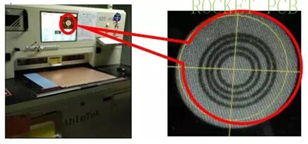
In the PCB production process, the commonly used method to detect layer deflection: at present, the commonly used method in the PCB making industry is to add a group of concentric circles at the four corners of the PCB production panel, set the spacing between concentric circles according to the requirements of the production panel layer deflection, and check the concentric deviation degree through the X-ray inspection machine or x-drill target machine in the PCB production process to confirm the layer deflection.
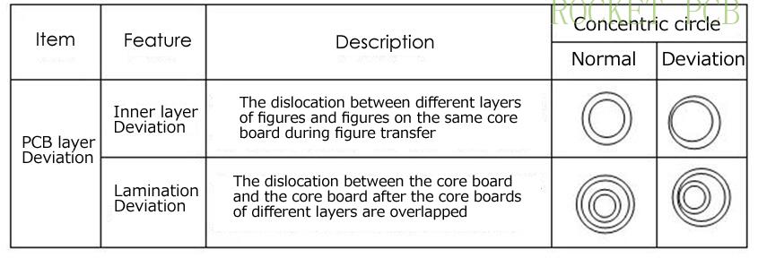
According to the layer of layer deviation and the process of layer deviation, layer deviation can be divided into inner layer deviation and laminated layer deviation (see the table below).
Classification of PCB layer deviation
Analysis of the causes of PCB layer deviation
The causes of inner layer deviation
The inner layer is mainly the process of transferring the figure from the film to the inner core board, so the layer deviation will only occur in the production process of the figure transfer, and the main reasons for the layer deviation are,
a. The inconsistent film inflation and contraction
b. The offset of the exposure machine
c. The improper operation of the personnel during the exposure process.
The main causes of PCB lamination layer deviation
a. Inconsistent expansion and contraction of the core board of various layers
b. The punch positioning hole is poor
c. The fusion is misplaced
d. The riveting is misplacede. And core boards sliding in the process of lamination.
Only by understanding the root cause of layer deviation can we better grasp the quality of PCB production, improve and promote the shortcomings of the PCB production process, and achieve good quality.


