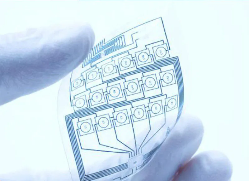
What are PCB\'s?
PCB is the abbreviation of the
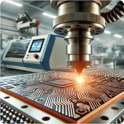
printed circuit board.
PCB uses conductive tracks, pads and other functions etched from copper sheets laminated on non-PCB to mechanically support and electrically connect electronic components
Conductive substrate. E-WasteE-
Waste or electronic waste is the remaining part of the PCB, components, PVC or plastic box/shell of old electronic equipment (such as TV, refrigerator), the dishwasher you throw out
It is one of the fastest growing waste on Earth.
Therefore, we must prevent it from becoming the largest type of waste produced on our planet.
According to a report on e-commerce
At the end of that year, 2017 were wasted. of-
Refrigerator, TV, mobile phone, computer, display
Toys and other products with batteries or wires around the world can be filled with 40-ton trucks end-to-
The end of the three-quarter highway across the equator is equivalent to the weight of 200 Empire State buildings or 11 Giza pyramids.
The United States has the highest nine digits in the world.
4 million tons, China produced the second highest Electronics
Total waste 7. 3 million tons.
The report also noted the total amount of e-commerce
Waste generated by 2017 will reach 65.
4 million metric tons.
What can we do to stop this?
The simple answer is, stop. consumption.
But it can take a long time to really take action.
The next important thing is to start recycling all the electronics and gadgets we left home. How? -
We can open the case/body of these devices, take out the PCB and reuse the assembly, crack the circuit board, so that we can build a new circuit on it.
But what about the plastic cover/case?
How do we recycle?
A 3D printer called ekcycle Cube®It can be 3D printed like other 3D printers, the only difference is that this filament is made from recycled Coke bottles.
Scientists have also been working on 3D printers, which use filaments made of plastic recycled from old electronic devices.
This Instructure will teach you, one of the most basic methods that can be used to reuse and recycle old PCB as well as components.
It may not be any different now, but it will certainly change in the future.
This is the beginning of reducing the output of electronic products. Waste.
Picture: PartsToolsTime30 minutess)
RequiredSolderingIMAGE: put the PCB in the vise or help the hand to turn the component side towards you.
If you are using the vise, start turning the lever so that the parallel vise of the vise holds the PCB in one place.
Image: Select the component you want to reuse.
Place the PCB vertically between the tiger claws of the vise, and the side of the pad is to you.
Outline the pads you want to design with a permanent marker.
This ensures that you do not have to refer to the other side of the PCB frequently.
Start to apply the tip of the soldering iron to the pad for a few seconds and apply some tin wire to the pad.
Now put the copper core on the pad and put the tip of the soldering iron on the pad.
Solder should start to remove from the pad and move to the copper core.
Once it\'s done, there won\'t be any solder on the pad & you can clearly see the lead of the Assembly.
Do this for all leads of this component.
Tip: start removing the big parts first.
This will make it easier to remove smaller components such as resistors and even SMD/SMT components.
Tip: tin core-
Solder core is a linear material used for description.
It is made of copper and it absorbs solder from the pad. Solder Pad-
The pads are also part of the soldering in the PCB. SMD/SMT-
Surface mounting equipment/surface mounting technology is the type of assembly that is usually welded by the machine.
They are very small in size, so can be installed in small PCB used in mobile phone, TV remote control, etcIMAGE: Once all solder pads are removed from solder pad, turn PCB, make the component side to you.
Gently pull out the assembly with pliers so that the Assembly leads do not twist or bend.
Do this for all large components on the PCB.
After removing the large parts of the PCB, you can start removing smaller parts such as resistors, Zener diodes, etc.
When you\'re done, you\'ll have various size components that you can use in future projects and hackers.
Image: Once all the components are removed, you can start the process of making a custom breakout board or even a custom board.
First mark the board with a permanent marker pen.
Use a hacksaw to cut the board into your requirements. E.
G: I\'m doing a relay breakout board.
So I cut the board so that my relay is mounted on the reduced board.
I also left some space to add the title pin as it was a breakout board.
Tip: when cutting the board, make sure to leave some copper path in order to add the header pin/output pin to it.
Tip: Breakthrough board-
It is a circuit board that allows you to access or connect pins of components or microchips: once the breakout board is cut into size, start to scrap the green layer printed on the copper path with a blade.
Once scrapped, you will be able to see the path of copper clearly.
This will now be the pad to weld the head pin or output pin to the pad in order to connect the breakout board.
Start drilling on these new pads.
Image: once you drill holes on the breakout board, you can weld the assembly into your respective slots, or you can weld the head pins into your respective slots to complete a custom breakout board.