


Design challenges of high speed HDI
With the increasing demand for the volume of information products, especially the development of mobile device products in the direction of continuous miniaturization, such as the current popular ultrabook products, even new wearable intelligent devices, must use HDI high-density interconnection technology to make the carrier board, and further reduce the size of the terminal design.
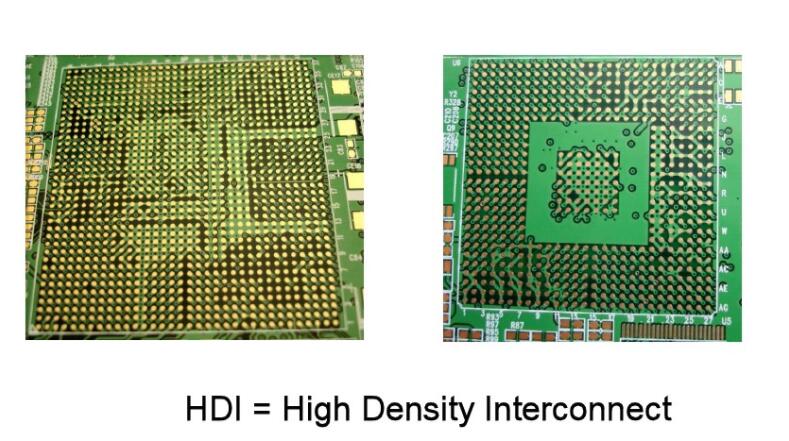
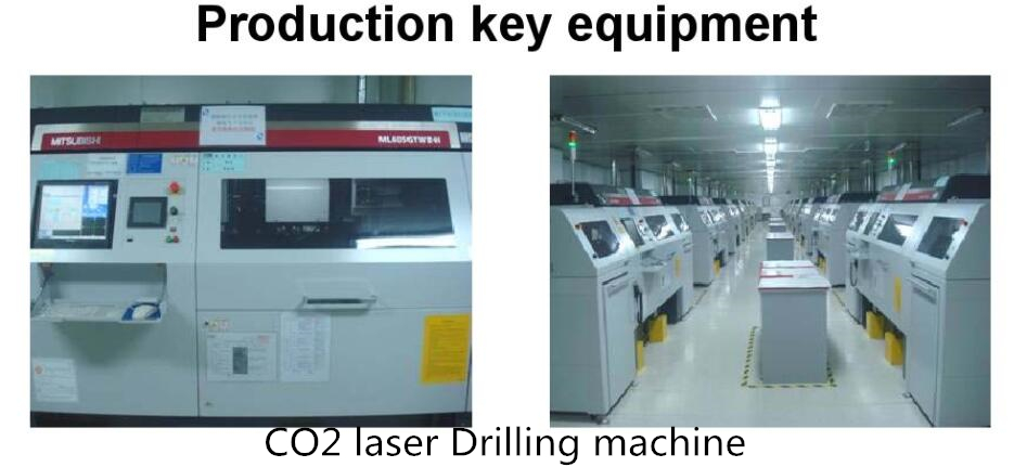
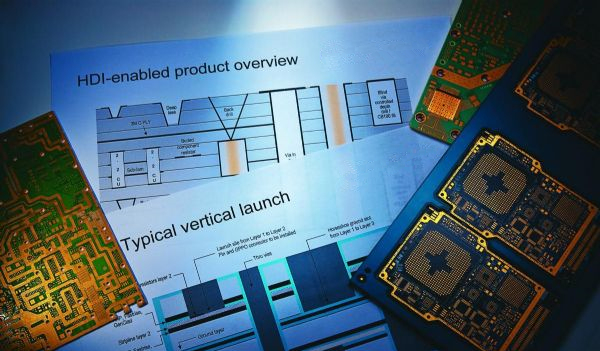
HDI (high density interconnect) is the high density interconnect technology, which is one of the technologies used in the printed circuit boards. HDI is mainly made by using the technology of micro blinds and buried holes. The characteristic is that it can make the circuit density of the electronic circuit distribution in the printed circuit board higher. Because of the increase of circuit density, the printed circuit board made by HDI can't use the general drilling method to make holes. HDI must use the nonmechanical drilling process. There are quite a lot of non-mechanical drilling methods. Among them, "laser hole forming" HDI high-density interconnection technology is the main matching hole forming scheme.
The application field of the HDI printed circuit board is quite wide. Electronic products such as mobile phones, ultra-thin notebook computers, tablet computers, digital cameras, automotive electronics, DV, etc. have all used HDI technology to reduce the design of the mainboard, and the benefits after reduction are quite large. Not only the terminal product design can leave more space in the mechanism for batteries, or more additional functional components, The cost of the product can also be reduced by importing HDI.
HDI was used in middle and high priced mobile phones in the early days, and now it is almost popular on all mobile devices
In the early stage, the products with the most HDI technology were mainly smartphones, which accounted for more than half of the consumption of HDI high-density circuit boards, while any layer HDI is a high-level HDI manufacturing process. The biggest difference between any layer HDI and general HDI circuit boards is that any layer HDI uses "laser" drilling to open each layer's interconnection design.
For example, the production method of any layer HDI can save about 40% of the PCB volume. At present, any layer of HDI has been used in iPhones and smartphones. By using a higher density integrated motherboard to reduce the product design thickness, the product design can use a lighter and thinner design style to the market. However, any layer HDI is made of laser blind holes, which are relatively difficult to process and manufacture in the circuit, and the cost is higher than that of general circuit boards. Currently, only high unit price mobile devices are used more frequently.
HDI printed circuit board is manufactured by the build-up method. The technology gap of HDI is the number of added layers. The more layers of the circuit, the higher the technical difficulty! The general-purpose HDI board can basically use one-time build-up. As for the high-level HDI board, it is manufactured by secondary or multiple times Build Up HDI technology. In order to avoid damage of HDI board high-density wiring caused by improper mechanical drilling, the hole forming process can use advanced PCB manufacturing technologies such as laser drilling, electroplate via filling, and hole stacking at the same time.
HDI requires a high density of circuit, the laser is required for drilling
First of all, the hole diameter of the circuit board made of HDI shall be less than or equal to 6mil, and the ring diameter of the hole ring shall be less than or equal to 10mil, and the layout density of the line contact shall be more than 130 points per square inch, and the line spacing of the signal line shall be less than 3mil.
There are many advantages of HDI PCB. Due to the highly integrated circuit, the area of the HDI board can be greatly reduced, and the higher the number of layers, the more the shrinkable board surface can be correspondingly increased. Due to the smaller size of the substrate, the area of the HDI application circuit board can be 2-3 times less than that of a non-HDI PCB design, but it can maintain the same complex circuit. Therefore, the material weight of the circuit board can be reduced.
As for the circuit design of specific blocks such as RF and HF, the multi-layer structure can be used. A large area of metal ground plane can be set in the upper / lower circuit of the main circuit, which will limit the EMI problem of high-frequency circuit caused by PCB to the inside of HDI board and avoid affecting the operation of other external electronic equipment.
The HDI board is lighter in weight and higher in circuit density, and the space utilization rate, in this case, is higher than that of the non-HDI board. However, the original high-frequency operation device will shorten the transmission distance of the signal line after HDI is adopted, which is naturally conducive to the signal transmission quality of the new SOC or high-frequency operation device.
Due to the better electrical characteristics, the transmission efficiency can be improved, and if HDI is used for more than 8 layers, it can basically obtain a better performance-price ratio than a non-HDI circuit board, which can also be used for terminal product design, to improve product performance and specification data performance, so that the product has more market competitiveness.
Key components with high pin number need HDI for product design
Especially for the FPGA components with too many pins, it is a great trouble for PCB wiring. For example, the most common GPU components at present, the number of pins is also toward more and more development. Most of them have used HDI printed circuit board for product design, and HDI is especially suitable for the design scheme requiring a high and complex connection.
Especially for the new generation of SOC or integrated chip, its highly integrated function leads to more and more IC pins, which greatly increases the difficulty of PCB design and connection circuit. HDI high-density circuit board design scheme can use the advantages of multi-layer interconnection and integration within the board to complete the connection of complex chip pins one by one, while laser blind hole production can make micro blind holes in the board, It can be perforated, staggered, stacked, or interconnected at any layer. The layout flexibility of the circuit is higher than that of the traditional PCB, and it also provides a more easy board design scheme for the integrated chip application scheme with a high pin number.
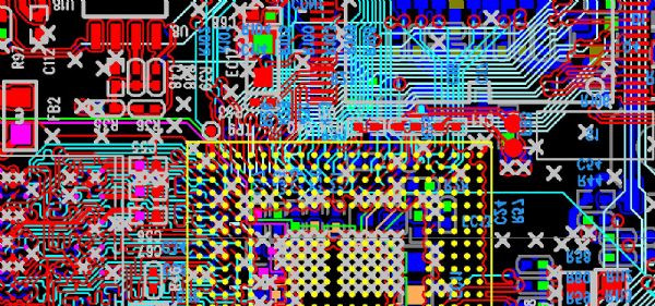
The design of HDI circuit board is more complex than that of PCB in the past, not only the circuit becomes closer, but also the design complexity of using different layers of circuit interconnection is greatly increased, the circuit becomes thinner and closer, which also represents the smaller of conductor cross-sectional area of the circuit, which will lead to the problem of transmission signal integrity will be more prominent, and PCB design engineers need to pay more attention to functional verification and error checking.
Especially in the face of highly complex design cases, such as in the development process, the possibility of electronic circuit design changes is quite high, and if the core components of the motherboard have FPGA or other components with a large number of pins, a little design change will cause a delay in the design improvement process, and how to reduce the occurrence of line deployment errors as much as possible in the design process with frequent changes, must be taken a design assistant tool for HDI high complexity circuit design. In particular, it must be matched with tools that allow changes in design specifications of any project to be immediately reflected in the development of the system under the design framework of FPGA logic design, hardware design, PCB Logic, and relevant design data can communicate with each other.
Avoid the design problem that the design board and the target chip cannot match
HDI circuit board design needs more careful product verification.
It is also because HDI PCB has greatly increased the circuit complexity, which will bring more design load to the original PCB wiring design work. In the actual development project, although the auxiliary development software can be used for rapid and positioning of wiring, in fact, it is still necessary to match the design experience of the developer to optimized component configuration and circuit layout. In order to simplify the design procedure of HDI PCB and reduce the lengthy development process, the development software automation, correspond to the pin-to-line connection, and the relative position of the pin is automatically changed.
In addition, HDI is often used in the design and application of high-speed components, especially in 3C or mobile devices, when they always have GHz level operation pulse, the trend of the mainboard circuit will also affect the EMI / EMC problems of the equipment in high-frequency operation. Generally speaking, the development software can be used to set the design parameters of timing rules and routing topology structure first, provide a referential constraint range for the development software, and then use the software verification function to carry out the local verification of the preliminary design. Of course, the local line verification of the development software is not the real line debugging it can only be used as the development reference at most. The actual design scheme must be verified by software several times before making reference design to verify the function of the HDI board.
There are many advantages to using software simulation verification. Basically, it can quickly find out the logic circuit that may make mistakes, check the points, lines, and check the blocks that may make mistakes in design. However, the speed of software simulation is quite fast. When there is no problem in software verification and simulation environment test, and then carry out entity verification on HDI PCB prototyping, HDI development cost can be greatly reduced.
Related Services from Rocket PCB: HDI printed circuit board, any layer HDI PCB prototyping, HDI PCB manufacturing. Solve your complex circuit board rapid prototype, HDI board quick turn around problem.


