


Analysis of back drilling PCB
PCB Engineers who do hardware know that the design of PCB vias is actually very particular. Today, I want to share the technical knowledge of via hole and back drilling in PCB.
In high-speed PCB design, high quality multilayer PCB is often used, and via-hole is an important factor in multi-layer PCB design.
Via hole in PCB is mainly composed of hole, pad area around hole and power layer isolation area
1. The influence of vias in high speed PCB
In high-speed PCB multi-layer board, signal transmission from one layer of interconnect to another layer needs to be connected via vias. When the frequency is lower than 1GHz, vias can play a good role in connection, and its parasitic capacitance and inductance can be ignored.
When the frequency is higher than 1 GHz, the parasitic effect of vias on signal integrity can not be ignored. At this time, vias show as discontinuities of impedance in the transmission path, which will cause signal integrity problems such as reflection, delay, attenuation, etc.
When the signal is transmitted to another layer via the via, the reference layer of the signal line is also used as the return path of the via signal, and the return current will flow between the reference layers via the capacitive coupling, which will cause the ground bounce and other problems.
2. Type of vias
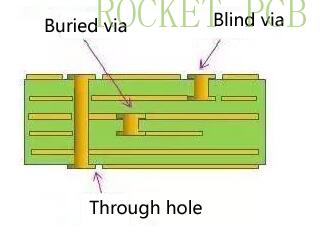
Via holes are generally divided into three categories: through holes, blind holes and buried holes.
3. Via hole design in high speed PCB
In the design of high-speed PCB, the seemingly simple vias often bring a lot of negative effects to the circuit design. In order to reduce the adverse effects caused by the parasitic effect of vias, we can try our best to:
(1) Choose reasonable via hole size. For the design of multi-layer general density PCB, it is better to select the via-hole of 0. 25mm/0. 51mm/0. 91mm (drilling / pad / power isolation area); for some high-density PCB, the via-hole of 0. 20mm/0. 46mm/0. 86mm can also be used, and the non via-hole can also be tried; for the via-hole of power supply or ground wire, the larger size can be considered to reduce the impedance;
(2) The larger the power isolation area is, the better. Considering the via hole density on PCB, it is generally D1 = D2 + 0. 41;
(3) As far as possible, the signal wiring on the PCB shall not be changed, that is to say, the vias shall be minimized;
(4) Using thinner PCB is propitious to reduce two kinds of parasitic parameters of vias;
(5) The pins of the power supply and the ground should be close to the vias. The shorter the lead between the vias and the pins, the better, because they will increase the inductance. At the same time, the power and ground leads should be as thick as possible to reduce the impedance;
(6) Place some grounding vias near the vias of the signal exchange layer to provide a short-distance circuit for the signal.
In addition, the length of via is also one of the main factors that affect the inductance of via. For vias used for top and bottom conduction, the length of vias is equal to the thickness of PCB. Due to the increasing number of layers of PCB, the thickness of PCB is often more than 5mm. However, in the design of high speed PCB, in order to reduce the problems caused by vias, the length of vias is generally controlled within 2. 0mm. For vias with a length greater than 2. 0 mm, the impedance continuity of vias can be improved to some extent by increasing the vias size. When the via-hole length is 1. 0mm or less, the best via-hole diameter is 0. 20mm ~ 0. 30mm.
1. What is PCB back drill?
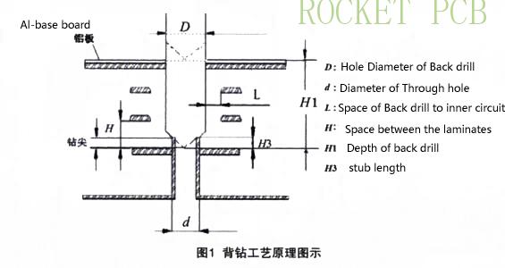
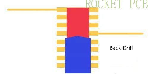
Back drilling is actually a special kind of deep drilling. In the production of multilayer PCB, such as the production of 12 layer PCB, we need to connect the first layer to the ninth layer, usually, we drill via holes (once drilled) and then electroless copper. In this way, the first layer is directly connected to the 12th layer. In fact, we only need to connect the first layer to the 9th layer. As there is no line connection between the 10th layer and the 12th layer, it is like a column.
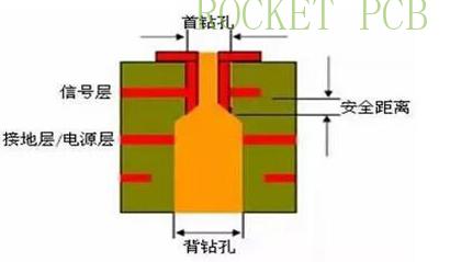
This column affects the signal path, which will cause signal integrity problems in communication signals. So the redundant column (stub) is drilled out from the opposite side (secondary drilling). So it's called back drilling, but generally it is not so clean, because the subsequent process will electrolyze a little copper, and the drill point itself is also sharp. So PCB manufacturers will leave a little bit. The length of this stub is called B value, which is generally in the range of 50-150um.
2. What are the advantages of back drilling?
1)Reduce noise interference;
2)Improve signal integrity;
3)The thickness of local board becomes smaller;
4)Reduce the use of buried blind holes and reduce the difficulty of PCB manufacturing.
3. What is the function of back drilling?
The function of back drilling is to drill out the via-hole section without any connection or transmission function, so as to avoid the reflection, scattering and delay of high-speed signal transmission, and bring "distortion" to the signal. The research shows that the main factors affecting the signal integrity of the signal system are not only the design, board material, transmission line, connector, chip package and other factors, but also the via-hole has a great impact on the signal integrity.
4. Working principle of back drilling production
When the drill needle is running in, the micro current generated when the drill tip contacts the copper foil on the base board surface will induce the height position of the board surface, and then run in according to the set depth of running in, and stop running in when it reaches the depth of running in. As shown in Figure 2:
5. Back drilling production process?
a. A PCB is provided, and a positioning hole is arranged on the PCB, and the positioning hole is used to drill and position the PCB;
b. The PCB after drilling is electroplated, and the positioning hole is subject to dry film sealing treatment before electroplating;
c. Making the outer layer figure on the electroplated PCB;
d. After the outer layer pattern is formed, the PCB is subject to pattern electroplating, and the positioning hole is subject to dry film sealing treatment before the pattern electroplating;
e、 A positioning hole is used for back drilling positioning, and a drilling knife is used for back drilling the electroplating hole to be back drilled;
f. After back drilling, the back drilling shall be washed to remove the residual drilling cuttings in the back drilling.
6. What are the technical characteristics of back drilling board?
1)Most backplanes are hard
2)The number of layers is generally 8 to 50
3)Board thickness: more than 2. 5mm
4)Large thickness diameter ratio
5)Large board size
6)Minimum diameter of general first drill > = 0. 3mm
7)The outer circuit is less, and most of them are designed by crimping hole array
8) The back hole is usually 0. 2mm larger than the hole to be drilled out
9) Tolerance of back drilling depth: + / - 0. 05mm
10) If back drilling requires drilling to layer M, the medium thickness from layer M to layer M-1 (the next layer of layer M) shall be at least 0. 17MM
7. What is the main application field of back drilling board?
Backplane is mainly used in communication equipment, large servers, medical electronics, military, aerospace and other fields. As the military and aerospace industries are sensitive industries, the domestic backplane is usually provided by research institutes and R & D centers of military and aerospace systems or PCB manufacturers with strong military and aerospace backgrounds; in China, the demand for backplane mainly comes from the communication industry, and now it is a growing communication equipment manufacturing field.


