


5G millimeter wave technology brings challenges to PCB manufacturing
5G is 100 times faster than 4G, the data capacity is 100 times higher, and the delay is less than 1 millisecond. What does this mean for PCB?
5G brings new design and manufacturing challenges to high-frequency PCB. To meet the 5G technical requirements, strict pattern design and complex materials are required. Therefore, the industry needs to adopt new imaging, detection, and measurement technologies to manufacture PCBs for 5G infrastructure and equipment.
5G infrastructure such as cellular base station, data server, high-performance computing system, and artificial intelligence increases the demand for fine line IC substrate board and high-level number (HLC) multilayer board (MLB). In terms of equipment, 5G antenna, camera module, and display driver increase the demand for flexible PCB, arbitrary layer high-density interconnection (HDI), and higher-density PCB with advanced HDI. All these 5 G-oriented PCB design requirements promote or exceed the limits of traditional PCB manufacturing technology.
Imaging technology
Some advanced manufacturing technologies are expected to provide the required imaging and detection capabilities and manufacture higher quality and more complex PCBs to meet the 5G technical requirements. These include direct imaging (LDI), automatic optical inspection (AOI), and automatic optical forming and repair. However, the manufacturing requirements of PCBs used in 5G infrastructure and 5G equipment are different.
In terms of 5G infrastructure, DI technology can realize the strict impedance control required for high-frequency 5G (such as millimeter wave), as well as the high precision and strict alignment accuracy of upper and lower layers on large panels, so as to meet the requirements for high-level MLB. High capacity anti welding (SM) DI technology can support large-size (up to 32 inches) and warped panels, while meeting the requirements of 5G for higher resolution and accuracy.
Automatic optical detection
Ideally, automatic optical inspection (AOI) should provide detection and measurement with little manual processing, and have detection as small as 5μM, which is a typical feature of HPC and data server in 5G infrastructure.
For 5G equipment, DI can provide high-quality imaging to meet the requirements of improved semi addition process (MSAP) or substrate-like PCB (SLP) production process for the fine circuit, accurate conductor geometry, high precision, and advanced scaling, while maintaining the highest effective production capacity and yield. With the increasing demand for 5G electronic products for smaller overall sizes, lighter weights, and higher functions, the importance of flexible printed circuit (FPC) components is increasing, which brings new challenges to manufacturing. The reel-to-reel DI system enables FPC manufacturers to use reel-based flexible materials while maintaining their integrity and minimizing frequent damage and deformation.
PCB AOI used in the equipment can be integrated with 2D laser blind hole measurement to measure the size of the blind holes, including top and bottom diameter, roundness and taper, and position. In addition, AOI integrated with automatic 2D linewidth measurement (Fig. 1) is the key to ensure accurate top and bottom measurement, so as to realize impedance control. At the same time, it is also very important for components such as 5G millimeter-wave antenna board.
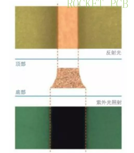
Figure 1. 2D measurement technology detects and measures the top and bottom trace guide of the PCB
In general, 5G PCB detection needs must address challenges such as low contrast material layers, transparent flexible printed circuits, laser blind hole detection, fast and accurate measurement for impedance control, and low cost of ownership. Some detection processes can also perform high contrast imaging on low contrast materials, so as to achieve complete detection without false positives.
There is another innovative process worth considering: automatic optical forming and repair. With this kind of optical repair technology, manufacturers can shape open circuits and short circuits with high speed and high quality when identifying advanced HDI (MSAP) PCB and IC substrate in the production line. This technology greatly reduces a scrap of plates and panels, saves time and manpower by eliminating manual repair links, and improves the overall quality and production yield. With the help of advanced automatic optical repair technology, manufacturers can improve the yield and quality in the large-scale production of 5G PCB, so as to enhance their competitive advantage.
Design and manufacture
Challenge the impact of 5G on PCB and IC board design and process, so as to achieve more accurate mass production. For example 28 GHz broadband base station.
As the world changes to 5G, a mini 5G base station is set every 100 meters in urban areas, which is installed on buildings, walls, roofs, traffic lights, and other facilities, in sharp contrast to 4G LTE, which is several kilometers away from large antenna towers. These 28 GHz broadband base stations require PCBs made of new materials, such as fast laminates with a low dielectric constant (DK, contrast), to increase wave speed and reduce transmission loss by up to 30%. 5G millimeter-wave requires impedance control as low as ± 5%, requires highly accurate PCB line size, and requires in PCB line measurement on all panels.
In this case, the production line shall include advanced Di for line pattern and anti-welding, as well as AOI for integrated 2D measurement of complex and high-rise digital boards.
5G server design
To realize 5G communication, it is necessary to combine local and central servers. This includes very large-scale data servers, which will create, process, store, and transmit massive data with the lowest possible delay. The included edge computing function processes real-time data created by sensors or users at the edge of the network (device level), rather than in the cloud. Running these servers and processes requires high-level PCBs, usually 12 to 22 layers, and high-performance data servers up to 30 layers. The transmission line needs strict impedance control to handle 5G high frequency.
In order to support high processing computing (HPC) units, the IC carrier board needs a new design with an area of up to 110mm×110mm to support larger chips and as low as 5 / 5μm Fine lines/spacing.
In order to achieve excellent defect detection, 5G server requires both Di and AOI to have a high depth of view (DOF) in the manufacturing process (Fig. 2). AOI integrated with 2D measurement and detection is also very important for strict impedance control. 5G Server Board also needs Di to realize high-precision and strict impedance control of upper and lower layer alignment, as well as anti-welding DI for a large board. AOI will ensure that the requirements for fully automated and high-capacity MLB are met. Finally, the automatic optical forming and repair system is conducive to low damage forming of short circuits and open circuits on PCB.
Figure 2. High depth of view (DOF) ensures excellent line quality and uniformity on different surface morphologies
The latest and next-generation 5G smartphones rely on MSAP / SLP, using extremely thin connection devices to effectively transmit signals and power to connected components while reducing power consumption. Flexible and rigid-flexible PCB is another requirement to realize smaller, lighter, and more functional equipment. More and more complex multiple-input multiple-output (MIMO) antennas are configured in 5G smartphones using an encapsulated antenna (AIP) to help achieve powerful functions.
Both MSAP / SLP and flexible PCB need laser hole detection in the AOI system to ensure the required quality and accurate positioning of connecting devices. Advanced Di system can ensure accurate and fine circuit patterning of MSAP / SLP board, high depth of field (DOF) of flexible and rigid-flexible combination board, and provide high production capacity to improve production. Finally, automatic optical forming and repair can form various defects found in the detection process, so as to greatly reduce the number of scrap plates.
Conclusion
With the help of advanced manufacturing technology, designers can build 5G infrastructure and equipment as needed to support new communication protocols and requirements. If appropriate manufacturing systems are adopted, such as laser direct imaging, automatic optical detection, and automatic optical forming and repair, designers will no longer need to worry about the low delay, high frequency, and complex and fragile materials. These technologies can not only be used to design and manufacture 5G components but also improve the yield in the large-scale production environment, which is very important for the deployment and use of 5G.


