


Terminology of printed circuit board-Part 2
PCB Common Terms
PCB (printed circuit board) is an important part of electronic products. The main function of PCB is to make all kinds of electronic components connect through circuit, play the role of conduction and transmission, and it is the key electronic interconnect of electronic products. Almost every kind of electronic equipment is inseparable from printed circuit board. The development level of PCB production reflects the development speed and technical level of national or regional electronic information industry to a certain extent.
Benefiting from the influence of the global PCB production capacity transfer to China and the booming downstream electronic terminal product manufacturing, China's PCB industry as a whole shows a rapid development trend. China has become the world largest PCB manufacturing base, spurred by strong demand growth in the downstream fields such as communication electronics, computer, consumer electronics, automotive electronics, industrial control, medical devices, national defense and aerospace. In recent years, the growth rate of China PCB production is significantly higher than that of the global PCB industry.
Definition of each layer in the PCB design
1 Signal layers
Altilum designer can provide up to 32 signal layers, including top layer, bottom layer and mid layer.The layers can be connected with each other through via, blind via and buried via.
(1) Top layer: also known as component layer, it is mainly used to place components. For double-layer PCB board and multi-layer PCB board, it can be used to lay wires or copper-clad.
(2) Bottom layer: also known as soldering layer, it is mainly used for wiring and soldering. For double-layer and multi-layer PCBs, it can be used to place components.
(3) Mid layers: there can be up to 30 layers or more layers, which are used to lay signal lines in multi-layer PCBs, excluding power lines and ground wires.
2 Internal plans
Generally referred to as the internal electric layer, it only appears in multi-layer boards. The number of PCB layers generally refers to the sum of the signal layer and the internal electric layer. As the same as the signal layer, the interconnection between the inner layer and the inner layer, and between the inner layer and the signal layer can be realized through through holes, blind holes and buried holes.
3 Silkscreen layers
A PCB board can have at most two silkscreen layers, namely the top silkscreen layer (top overlay) and the bottom silkscreen layer (bottom overlay), which are generally white. They are mainly used to place printed information, such as the outline and mark of components, various annotation characters, etc., which are convenient for component soldering and circuit inspection of PCB.
(1) Top overlay: used to mark the projection outline, label, nominal value or model of components and various annotation characters.
(2) Bottom overlay: the same as the top silkscreen layer. If all the silkscreen layers marked on the top have been included, the bottom silkscreen layer can be closed.
4 Mechanical layers
The mechanical layer is generally used to place the indicative information about the PCB making and assembly method, such as the outline dimension, dimension mark, data, via information, assembly instructions and other information of PCB. This information varies according to the requirements of the design company or PCB manufacturer. The following examples illustrate our common methods.
Mechanical 1: Generally used to draw the frame of PCB as its mechanical shape, so it is also called the shape layer;
Mechanical 2: We use it to place PCB machining process requirements table, including size, PCB board, PCB board layer and other information;
Mechanical 13 & mechanical 15: the body size information of most components in ETM library, including the three-dimensional model of components; for the sake of page simplicity, this layer is not displayed by default;
Mechanical 16: the occupying area information of most components in ETM library can be used to estimate PCB size in the early stage of the project; for the sake of page simplicity, this layer is not displayed by default and the color is black.
5 Mask layers
Altium designer provides two types of mask layers: the solder mask and paste mask. There are two types of mask layers: the top layer and the bottom layer.
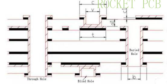
Through hole, blind hole and buried hole
The devices of mobile phone can only be arranged on the upper and lower sides of PCB (the latest technology has been able to put passive devices such as capacitors directly inside PCB-Embedded PCB). The wiring needs to pass through different layers of PCB, so the signal must be changed to different layers through a series of vias.
Through hole: a hole passes through all layers of PCB from top to bottom.
Blind hole: that is to say, one section of the hole is on the surface and the other end is on an inner layer of PCB.
Buried hole: that is to say, the two ends of the buried hole are in the inner layer of PCB relative to the blind hole.
Generally speaking, both ends of the through hole can be seen on the upper and lower surfaces of the PCB, and the blind hole can only see one end of the hole on one surface, while the buried hole can not be seen. In order to improve the performance of through-hole, blind hole and buried hole are usually electroPCB boardd and filled with copper / resin to form solid hole, which is invisible to the naked eye.
3 PCB stage/level
The so-called stage is related to the number of times the inner PCB board is pressed together, which is also equivalent to the number of layers through the blind hole. Take 8-layer PCB board as an example. If all vias are through holes, they are called through-hole board, i.e. 0-stage PCB boards. If there are 1-2 / 7-8 blind holes in addition to through holes, it is called 1-stage PCB board. In addition, there are 1-3 / 6-8 blind holes, which are called 2-stage PCB boards.
The blind hole of the third-stage PCB board of the 10 layers is 1-4 / 7-10. The higher the stage is, the more flexible and free the PCB is, the better the electrical performance index will be, but the cost will be very high. At present, the mainstream high-end mobile phone basically adopt any-stage. For example, iphone adopts the N-layer and N-stage technology, that is to say, any two levels can be drilled. All the processes are laser drilling, with high precision and high price.
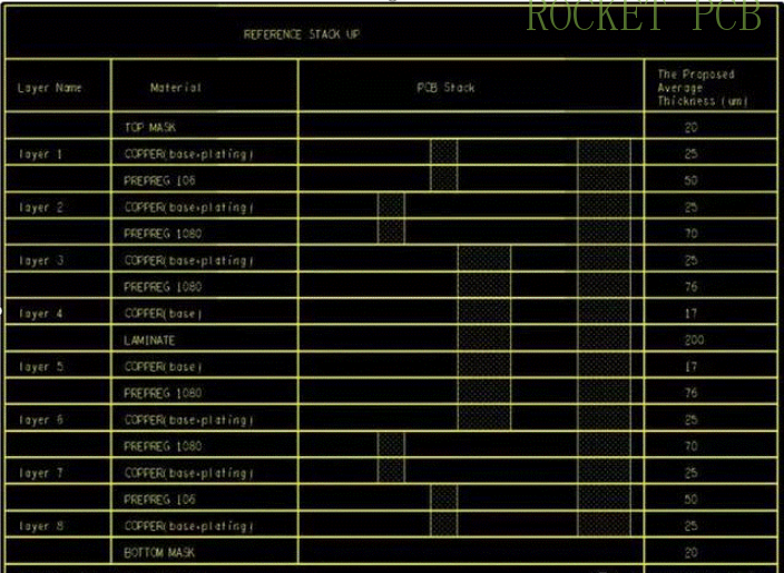
4 Copper thickness
Copper thickness is copper clad thickness. In PCB design and PCB processing, oz (ounce) is commonly used as the unit of copper sheet thickness. The definition of 1oz copper thickness is that the weight of copper foil within 1 square foot area is one ounce, and the corresponding physical thickness is 35um; the corresponding 1 / 2oz and 1 / 3oz are 17.5um and 11.7um respectively. The following figure shows the common copper-clad thickness of 8-layer 2-step PCB board. The surface layer is 20um and the inner layer is 25um.
5 Rigid and flex
Our common PCBs are rigid PCB boards, which protect the devices on the board from mechanical stress to a certain extent, commonly known as rigid PCB boards.There is also a flexible printed circuit board called FPC (flexible printed circuit), especially the connection between LCD and main board, the connection between camera module and main board connector, etc. The advantage of FPC is its flexibility, arbitrary shape and bendability, but it should be noted that its strength is not enough and it is easy to be affected by mechanical stress.
6 Electrical performance of PCB
The current carrying capacity of PCB depends on the following factors: line width, line thickness (copper foil thickness), allowable temperature rise. Commonly used pcb board production length unit conversion: Inch, mil, mm, cm
1mil=0.0254mm=25.4μm 1mm=39.37mil 1inch=1000mil=25.4mm
7 Common performance indexes of PCB substrate
TG: glass transition temperature, which is divided into tg130-135 degrees (normal), tg150 degrees (medium TG), tg170-175 degrees (high Tg).
Dielectric constant (DK): FR4 is usually between 3.9-4.6, which should be considered in impedance calculation;
Coefficient of thermal expansion (CTE): performance index of PCB board deformation at high temperature
Leakage tracking index (CTI): parameters related to resistance to high voltage breakdown
Ion migration (CAF): affecting the reliability of boards
Loss tangent (DF): parameter related to loss of signal on board
China has a healthy and stable PCB domestic demand market and a significant PCB manufacturing advantage, attracting a large number of foreign capital enterprises to shift their PCB production focus to mainland China. As a basic electronic component, PCB industry is mainly built around the downstream industrial concentration area. In 2019, the number of domestic PCB industry enterprises is about 2300, mainly distributed in the Pearl River Delta, Yangtze River Delta and Bohai Rim region, which have strong economic advantages, location advantages and talent advantages. However, in recent years, affected by the rising labor cost, some PCB enterprises have gradually transferred their PCB production bases to inland areas, such as Jiangxi, Hunan, Anhui, Hubei, etc., in order to alleviate the operating pressure brought by the rising labor cost.


