


What Are The PCB Fabrication Processes For Bare Boards?
The process of creating PCB is a very technical one and has many details incorporated within it. A single flaw in the design or any other step could cause the entire PCB to be useless. Hence taking care of the whole process is very important.
PCB fabrication means manufacturing the bare boards for the PCBs to be further printed and designed to be put to the purpose. PCB bare boards are created after many steps are undertaken. Here, you will get a detailed insight regarding PCB fabrication.
Create circuit image
It is imperative to create image data so the board may be designed accordingly. There are two ways in which this image data is created, and both of them are discussed below:
1. Photo tool
The process of photo tooling is used to create the circuitry images, and this is quite a suitable process when there is bulk production of PCBs. A photoplotter works in an exact manner and makes the images on the given film, and then the image is printed on the board.
2. Direct imaging
Another method of circuit image creation task is using laser printers to create the circuit image rather than photo tools. It gives a very perfect and precise outcome but is an expensive technique.
Layers of the circuit board
In the next step, a circuit board of various layers is created; these layers comprise metal conductors followed by dielectric material made from resin and FR-4. FR-4 is a fiberglass material that is placed between copper foil. FR-4 proves to be the best material used for PCB fabrication.
A double-sided circuit board is created and contains multiple layers stacked together. All the layers must be of the correct dimensions keeping the weight controlled for the copper used.
Creating the inner layers of the circuit
There are inner layers that need to be provided with the circuitry images, which form the initial step in PCB fabrication. A material with photoresist characteristics is chosen first, and the core, which has the copper foil, is covered with such material. Now selecting a photo tool or the direct imagining process of laser, ultraviolet light is passed over the material.
The points where hardening of photoresist material is needed only those areas are subjected to this ultraviolet light so that the photoresist material hardens at such points. Then the rest of the material is removed from the copper foil later.
After this, only the hardened photoresist portions are left behind, and the core areas of copper are even removed. The final layer is then inspected for any flaws, and if detected, those are addressed immediately.
Laminate stacked together
The next step is where lamination is carried out. The layers of copper foil cover the board from all sides. These layers also have a fiberglass sheet incorporated in between. This fiberglass material has resin, and during the lamination process, when it is subjected to pressure and heat, the material melts down to bond the layers together upon cooling.
These laminated layers, upon cooling, create a proper circuit board. This process requires a lot of attention since it is one of the most sensitive processes of making the PCB.
Drilling holes
The process of drilling holes is the next step, where holes are drilled in the board so the components can be placed over it with wires being passed around. After the drilling process is carried out, the entire board is cleaned.
This is very important to ensure that no debris is left behind during the drilling process and that there is no leftover resin from the previous step. These through holes are plated with the drilling process. After the board is cleaned, it is subjected to further electroplating, and a fine layer of copper is introduced to layer the board as part of the PCB fabrication process.
Building the circuitry of the bottom and top layers
The central layer was manufactured using a photoresist material, and the same material will now be used in the PCB fabrication process to create the top and bottom layers of the PCB.
The surface of the board used for the top and bottom parts is once again covered with the same photoresist material, and it is then subjected to UV light. This time the circuitry patterns are not exposed to UV light.
Using a chemical, all those unexposed areas of photoresist material are removed, and then the task of tin plating is carried out. The tin plating adds protection to the board, and after the final plating is done, leaving the circuitry patterns, the rest of the areas with tin and copper are also removed. Now you will see the thru-holes, traces, and pads where the components can be fixed.
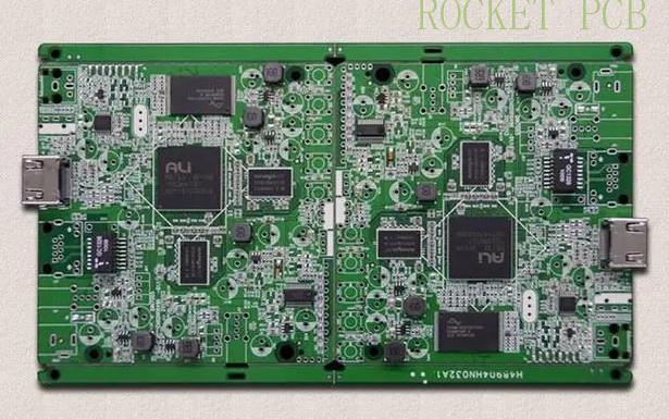
Surface preparation, silkscreen, and solder resist
In order to add more protection to the circuit board, a soldering mask is applied to the entire board except for the metal points. This is done in the same way as the photoresist material is applied. Also, silk screening is carried out, followed by a surface finish.
Surface finishing requires the board to be dipped into a molten solder material. After being submerged, it is subjected to a hot air blast that eliminates excessive solder and leaves behind a finished surface of the board.
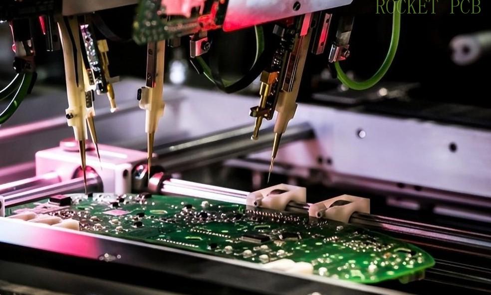
Assembly, inspection, and testing
The last step of PCB fabrication is where the board is now assembled and tested for any flaws if it exists. The process comprises continuous testing and inspection of the board, ensuring that no shorts will occur. In case if the board is defaulting somewhere, it is subjected to rejection and is no longer used.
Its application is very sensitive; hence there is no room for a single defect. Therefore, the process of assembling and inspection is very detailed so that it is adequately tested.
Conclusion
At Rocket PCB, you can always rest assured that all the PCBs we create are fabricated in the finest way, and you get the best final product ready to use for your components. We leave no room for any flaw in the PCBs we manufacture.
We always ensure that the detailed PCB fabrication process is undertaken by us from scratch using the finest quality material used in layers and the entire process. We have an experienced team looking after the whole process, and you will always have defect-free circuit boards ready to use for your equipment without any hassle. So, get in touch with us today and have your PCBs prepared in no time.


