


What are the common PCBA inspection methods?
Inspection is a key step in all PCB production processes. It can detect PCB defects in order to correct them and improve overall performance.
Inspection of the PCB can reveal any defects that may have occurred during manufacturing or assembly. It can also help uncover any design flaws that may exist. Checking the PCB after each stage of the PCB processing process can find defects before moving on to the next stage, thus avoiding wasting more time and money to buy defective products. It can also help find one-time defects that affect one or more PCBs. This process helps to ensure consistency of quality between the board and the final product.
Without proper PCB inspection procedures, defective boards may be handed over to the customer. If a customer receives a defective product, the manufacturer may suffer from warranty payments or returns. Customers will also lose trust in the company, damaging the company's reputation. This situation can lead to missed opportunities if customers move their business elsewhere.
In the worst case, if a defective PCB is used in a product such as a medical device or a car part, it can cause injury or death. Such problems can lead to serious reputation damage and expensive litigation.
What is PCB inspection?
In order to ensure that the PCB can operate as expected, the manufacturer must verify that all components are assembled correctly. This is accomplished through a series of technologies, from simple manual inspection to automated testing using advanced PCB inspection equipment.
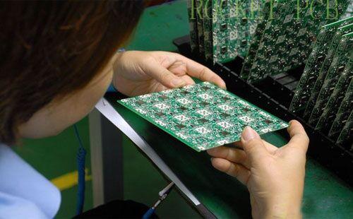
Manual visual inspection
Manual visual inspection is a good starting point. For relatively simple PCBs, they may only be needed.
The simplest form of PCB inspection is manual visual inspection (MVI). In order to perform such tests, workers can view the board with their eyes or with magnification. They compare the board with the design documentation to ensure that all specifications are met. They will also look for common default values. The type of defect they are looking for depends on the type of circuit board they are checking and the components on it.
It is useful to perform MVI after almost every step in the PCB production process, including assembly.
Inspectors inspect almost every aspect of the board and look for common defects in every area. A typical visual PCB checklist may include the following:
·Make sure the thickness of the circuit board is correct and check the surface roughness and warpage.
·Check whether the dimensions of the components meet the specifications, and pay special attention to the dimensions related to electrical connectors.
·Check the integrity and clarity of the conductive pattern, and check solder bridging, open circuit, burrs and voids.
·Check the surface quality and then check for dents, dents, scratches, pinholes and print traces and other defects on the pad.
·Verify that all through holes are in the correct position. Make sure there are no omissions or incorrect holes, the diameter is in accordance with the design specifications, and there are no gaps or summaries.
·Check the base plate for tightness, roughness and brightness, and check for bulge defects.
·Evaluate coating quality. Check the color of the plating flux and whether it is uniform, firm and in the correct position.
MVI has several advantages over other types of inspection. Because of its simplicity, it is low cost. No special equipment is required except for possible enlargement. You can also do these checks very quickly and easily add them to the end of any process.
The only thing needed to carry out such inspections is to find professional staff. This technique may help if you have the necessary expertise. However, it is essential that employees use the design specification and know what defects need to be noted.
The function of this method is limited. It cannot check components that are not in the worker’s view. For example, hidden solder joints cannot be checked in this way. Employees may also miss some defects, especially small ones. Using this method to examine complex boards with many small components is particularly challenging.
Automated optical inspection
PCB inspection machine can also be used for appearance inspection. This method is called automatic optical inspection (AOI).
The AOI system uses multiple light sources and one or more stationary or cameras for inspection. The light source illuminates the PCB from all angles. The camera then takes a still image or video of the circuit board and compiles it to create a full picture of the device. The system then compares the captured images with information about the appearance of the board obtained from design specifications or approved complete units.
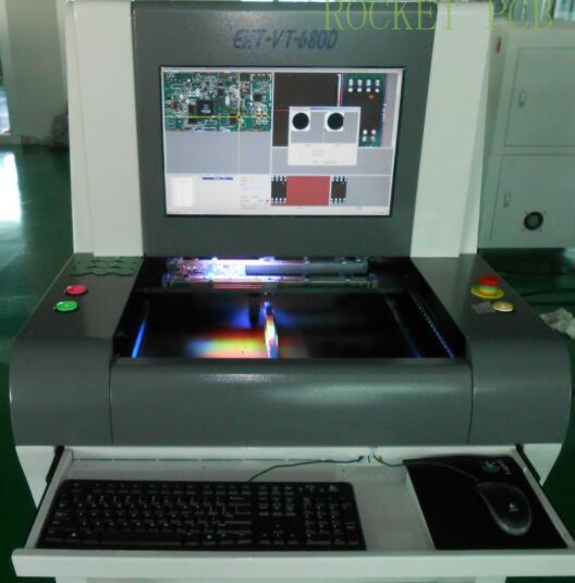
Both 2D and 3D AOI devices are available. 2D AOI machines use color lights and side cameras from multiple angles to check components whose height is affected by them. The 3D AOI device is relatively new, which can measure the height of components quickly and accurately.
AOI can find many of the same defects as MVI, including nodules, scratches, open circuit, solder thinning, missing components, etc.
AOI is a mature and accurate technology, which can detect many faults in PCB. It is very useful at many stages of the PCB production process. It is also faster than MVI and eliminates the possibility of human error. Like MVI, it cannot be used to check out of sight components, such as connections hidden under spherical grid arrays (BGA) and other types of packaging. This may also not be effective for PCBs with high component concentrations, as some of them may be hidden or obscured.
Automatic laser measurement
Another method of PCB inspection is automatic laser test (ALT) measurement. ALT can be used to measure the size of solder joints and solder deposits, as well as the reflectivity of various components.
The ALT system uses a laser to scan PCB components and make measurements. When light is reflected from the components of the board, the system uses the position of the light to determine its height. It also measures the intensity of the reflected beam to determine the reflectivity of the component. The system can then compare these measurements to the design specifications, or to boards that have been approved to accurately identify any defects.
The ALT system is ideal for determining the amount and location of solder paste deposits, which provides information about alignment, viscosity, cleanliness, and other attributes of solder paste printing. The ALT method provides detailed information and can be measured very quickly. These types of measurements are usually accurate, but can be disturbed or shielded.
X-ray examination
With the rise of surface mount technology, PCB becomes more and more complex. Today, circuit boards are denser, have smaller components, and include chip packages such as BGA and chip level packaging (CSP), through which hidden solder connections are not visible. These functions bring challenges to visual inspection such as MVI and AOI.
To overcome these challenges, X-ray inspection equipment can be used. The material absorbs X-rays according to its atomic weight. Materials can be distinguished by the fact that heavier elements absorb more and lighter elements less. Solder is made of heavy elements such as tin, silver and lead, while most of the other components on a PCB are made of lighter elements such as aluminum, copper, carbon and silicon. As a result, solder is easy to see during X-ray inspection, while almost all other components (including substrate, lead and silicon IC) are not visible.
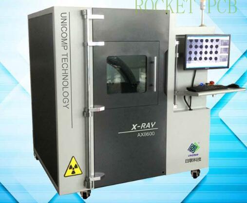
Instead of being reflected like light, X-rays pass through an object to form an image of the object. This process enables the perspective of chip packages and other components to examine solder connections beneath them. X-ray inspection also allows you to see the inside of the solder joint to detect bubbles that cannot be seen with AOI.
The X-ray system can also see the heel of the solder joint, which is covered by the lead wire during AOI. In addition, when X-ray examination is used, no shadow will enter. Therefore, X-ray inspection is very effective for circuit boards with dense components. X-ray examination can be performed manually or automatically with the X-ray system.
X-ray inspection is an ideal choice for more complex circuit boards and has some functions that other inspection methods do not have, such as the ability to penetrate chip packages. It can also be used to check the PCB with dense packing, and can check the solder joint in more detail. It’s a bit more expensive, and it’s probably a bit more sophisticated. Investment in X-ray inspection equipment is only required when there are a large number of dense circuit boards with BGA, CSP and other such packages.


