


Advantage and applications of Copper Inlay PCB
Copper inlay PCB can release heat from heater elements mounted on an electronic circuit board through copper inlays to a bottom side heat sink.
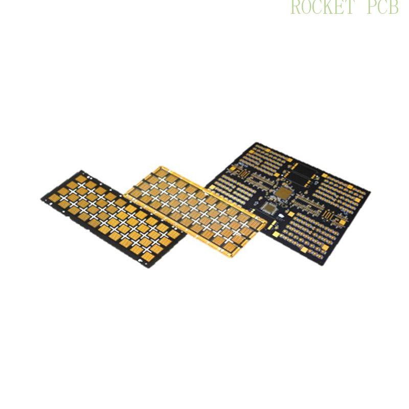
In Metal Inlay Technology a massive copper element is pressed into the printed circuit board and serves to dissipate the heat of an electronic component through the printed circuit board. The heat-emitting component can be connected directly to the metal inlay. Copper inlays with a minimum diameter of 5mm and a thickness of 0.8-2.5 mm are used primarily for this. Depending on their shape and dimensions, the metal inlays are inserted fully or semi-automatically.
Any shape can be chosen for the metal inlays. The required recesses in the printed circuit board are produced by milling or drilling. Mounting holes up to a diameter of 6.35 mm can be produced during the first drilling procedure and are therefore cost-efficient.
The use of metal inlays allows substantial improvement of the thermal conductivity (through the printed circuit board) compared with conventional thermal vias.
Copper Inlay PCB applications
Copper Inlay PCB is well recognized in Japan and is becoming a trend for Heat Dissipation PCB.
Copper Inlay PCB is widely used in many industry fields, and especially used in automotive parts which are important for human safety.Motor controls (ECU), ABS, ESP, start-stop systems.
In addition,Copper Inlay PCB can be widely used in Humanoid Robot,High Efficiency.
industrial electronics: inverter and rectifier, power electronics, control electronics,Server Power Supply and Battery Management System.
lighting technology: LED lighting, special projectors and cinema technology.
Due to higher and versatile performance of parts, heat generation of parts increases, and countermeasure for heat dissipation becomes more important in order to maintain product performance and life.
Also, miniaturization of parts makes it difficult to get natural heat dissipation from parts themselves. We need to design PCB so that heat is dissipated through traces on PCB.
Advantage of Copper Inlay PCB
optimal heat dissipation through direct connection of the component to the metal inlay.
Compared to Aluminum Base PCB, more flexible design is possible because we can use multiple layer PCB, and both sides parts mounting board.
Increasing circuit efficiency by more flexibility of part placement
Miniaturization
Implementation of cost effective solution for heat dissipation
Compared to Aluminum Base PCB, reliability of solder connecting part will improve because linear expansion coefficient of copper is lower than that of Aluminum.
It is possible to satisfy QCD(Quality/Cost/Delivery) such as better reliability by eliminating fastening screw process for heat generating parts, reducing cost and reducing assembly process.
It is possible to use same heat dissipation structure for surface mount and Lead parts.
optimal heat conduction through the printed circuit board: the continuous copper path enables excellent conduction from the heat source to the heatsink
combination with other technologies possible, e.g. heatsink, semiflex etc.
electrical connection of the metal inlays possible - also to the inner layers
freedom to choose the geometry of the metal inlays
fully automatic mounting of round metal inlays, semi-automatic mounting for other shapes
very good planarity of the inlay to the reference layer (component or heatsink side)


