


Cost factors of HDI PCB
In this article, we will introduce the cost and manufacturing best practices of HDI PCB, and the reasons for using HDI in some applications. HDI board has four main problems: HDI PCB material, layer and lamination, vias in HDI board, and optimal trace and space.
The implicit economy of HDI PCB
In PCB manufacturing, the number of laminations often indicates more cost. It is obvious that a 6-layer board is certainly more expensive than a 4-layer board.
As the circuit design becomes more and more complex, will you simply add layer by layer and make the holes smaller and smaller? Why should we design a high through-hole aspect ratio and tight hole copper spacing instead of turning to a buried through-hole structure and achieve a larger hole to copper gap? Easy-to-process low- thick diameter ratio, e.g. less than 8:1. The advantage of HDI PCB design is to achieve higher line density in limited space, increase design efficiency and reduce the cost of a high multi-layer board.
HDI board design is not just layer and lamination
Simply increase the number of layers, make everything smaller, and think that the manufacturer only needs to deal with it, which is a lack of thinking. If you focus on the lowest installation cost, you will have to carefully evaluate the cost of HDI construction and the cost of not using HDI under a certain degree of circuit complexity.
Yes, multiple laminations are more expensive than single laminations, but this is only one factor to consider when conducting a comprehensive cost-benefit analysis when developing laminations. First, let's distinguish between HDI prototype manufacturing and production operation.
HDI prototype manufacturing and standard manufacturing
When a workshop superior to HDI prototype manufacturing quotes and accepts orders for 10pcs boards, the manufacturer certainly has the responsibility to do it well, even if it may be on the edge of process tolerance. A 6-layer board with 3mil drilling and wire gap may be easy to produce, but the same situation will be another story on the 12th layer, which involves product yield. Maybe the PCB manufacturer must make 20 boards to produce acceptable 10 boards, so the work must be run twice. If the delivery is delayed, what is the cost of the new product development cycle and introduction? The manufacturer will have to absorb 50% of the waste and charge customers. If the customer needs some changes to upgrade the version, similarly, the manufacturer will adjust the price to compensate 50% of the production. The customer may have no choice but to pay for the price increase or delay the development. At this point, too much has been invested in design to start over.
The yield of standard manufacturing is also affected, and there will be some additional assembly losses. apparent, Output is the most important cost consideration in PCB.
The manufacturing cost of a 10 layer board using a build-up 2 + 4 + 2 structure is different from that using 5 core 4-Z interconnect structure. In terms of output improvement and yield, the core board pressing structure has more advantages.

When is the HDI PCB design worth the extra cost?
Suppose the customer asks to build a 12 layer board, which contains several BGAs and 12 layers×15 ball matrix, with very small spacing. This is a through-hole single laminate design of an old customer. Its thickness is about 0.093 inches. The design requires that we can drill the smallest hole, which is beyond the hole we should normally drill, but the gap between the hole and copper is only about 3 mils. Although we can make them, it is impossible to produce them with any reliability.
If BGA with ball spacing less than 0.5 mm is involved, you should always consult the circuit board manufacturer before starting the layout.
Explore how to best build manufacturability. There are 12 layers of 2.5 mils to 3 mils of wiring inside the BGA matrix. This design can easily be redefined as an eight-layer 2-4-2 HDI board with two continuous laminations. All drilling to copper criticality of the HDI structure will disappear. The wiring can be healthy 4 mils to 5 mils or even wider because it is not necessary to thread between adjacent through holes in the pad. Easily produce a circuit board with excellent yield and less than four layers.
Factors affecting HDI manufacturing cost
HDI board has four main problems: HDI PCB material, layer and lamination, vias in HDI, and optimal routing and space.
1. Material performance and cost of HDI PCB
HDI PCB materials from different material manufacturers may have almost the same characteristics, but the processing difficulty of one material may be more or less than that of another material, especially for HDI technology. Their raw material prices have little correlation with their manufacturing difficulty and plate output while manufacturing output drives profits.
For HDI manufacturing, the material must have three key qualities.
1, it must be dimensionally stable, and this quality of course applies to non-HDI structures. All materials shrink and stretch to some extent during the manufacturing process, and the pattern must be scaled to compensate.
2, the material must be easy to process: for HDI, this means that it can laser drill without a problem.
3, the material must be able to withstand multiple laminations.
Taking N4000-13 SI, FR408HR, and Megtron 6 as examples, the manufacturability comparison is limited to laser drilling.
The highly concentrated energy is directed into a focused beam in a specific area, which is absorbed by the material until evaporation. The energy must be carefully controlled to ablate the material to form holes without damaging the underlying landing pad. However, the dielectric components absorb energy at different rates, so the manufacturability of N4000-13 SI, FR408HR and Megtron 6 is different.
Consult your board manufacturer at the beginning of the design to determine the materials that can achieve the best balance between price, manufacturability and performance according to your structure. Broadly speaking, the manufacturing yield of the HDI design of the specified material depends on whether the material is dimensionally stable, whether it is easy or resistant to copper migration (such as conductive anode wire (CAF) growth), whether it can withstand multiple laminations, and whether the laser drilling effect is consistent. A circuit whose response remains relatively flat in its frequency range will faithfully propagate the signal without distortion. The dielectric constant (DK or ER) of the material decreases with the increase of frequency. The high-speed digital signal involves a wide frequency band, so it is easy to cause distortion due to the impedance change caused by the change of DK of circuit board material with frequency. The change of loss factor (DF) of circuit board material with frequency will also reduce signal integrity. Compared with materials with higher DK and DF, materials with lower DK and DF and little change in the frequency domain of the whole circuit propagate signals faster and can better maintain signal integrity.
2. When considering layers and laminations, please keep the following questions in mind:
have you planned to reduce EMI? Have you decided on your routing density? What is the total number of consecutive laminations? Did you minimize your laminations?
3. The type and structure of vias affect the cost of HDI board
3.1 mechanical drilling or laser drilling
The via quality of HDI PCB is directly related to the cost of electroplating and HDI PCB. Mechanical drilling and laser drilling are the most commonly used through-hole drilling formats. Mechanical drilling is a traditional drilling technology. Due to its economic benefits, it is still used as an effective drilling method for through holes and blind holes. The precise production of blind holes requires special techniques, such as drilling depth control, to ensure that blind holes can be formed repeatedly. Compared with laser drilling, mechanical drilling has a lower capital cost. But in the case of operating costs, it is different. In addition, the cost of damaged drilling is higher because it requires additional metallization and additional operating costs. Therefore, laser drilling is preferred for key drilling and mass production.
If we compare the cost of drilling a through-hole, mechanical drilling is more economical than laser drilling. However, considering the high accuracy of 1000 through holes, the consistency of drilling quality and the cost of high-speed machining, laser drilling is economical. How much is a 6mil drill more expensive than a 10mil drill. If you have the opportunity to reduce or eliminate mechanical drilling and switch to laser drilling, you can save a lot of direct production costs.
3.2 via structure
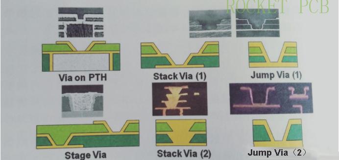
Let’s continue to discuss vias. The manufacturability is mainly related to the through-hole structure. Before proceeding to the next project, please answer the following questions: do you comply with the design guidelines for microvia aspect ratio? Do you stack or stagger microvias?
3.2.1 conductive or non-conductive hole filling
The next cost factor to consider is the choice between conductive or non-conductive hole filling processes. Are there vias under surface mount components that need to be filled, capped or plated? This is expensive because it requires two plating steps and two drilling steps. Our drilling will be filled separately from the conventional through holes on the plate, and any additional steps will mean additional cost. In this case, we will return to the process twice, and the cost includes time and money, drilling and electroplating.
The ultimate purpose of hole filling is to help assemble and form good solder joints. It works very well. Please note the additional cost and time that comes with it. If you can choose between offset laser drilling holes and pad through holes, I will choose laser drilling holes instead of mechanical drilling.
It can electroplate laser drill and through-hole mechanical drill at the same time. Pad design is not only another step in the process, but also challenges the manufacturing registration system. If you use through-hole mechanical drilling instead of laser drilling to achieve through-hole in pad, additional non-conductive filling process steps are required. The use of non-conductive filler is more expensive than electroplated laser drilling closure.
3.2.2 laser microvia aspect ratio
The key dimensions of laser microvias are pad size, laser drilling size and dielectric extrusion thickness. You must define your laser drilling size in proportion to the finished extrusion thickness in order to correctly electroplate the through hole. Although the size of laser drilling can become very small. But remember that they only go through one floor. Many manufacturers make 2 mil laser holes, but electroplating 2 mil holes will have problems due to the aspect ratio.
The aspect ratio of 1:1 is not optimal. You want to keep 0.8:1 to ensure good plating. The shape of the vias is important for the proper flow of the plating solution and plating or filling. If you must have a buried hole, you need to choose between staggered or stacked vias.
3. 2. 3 staggered and stacked vias
Staggered through holes essentially mean fewer process steps. We do not have to fill the laser drill with copper because the second laser drill will not fall on the first laser drill. Microvias filled or closed by plating usually occur in special plating tanks. It plated the micro holes drilled by laser from the bottom of the through hole to the top of the through hole until the hole was completely filled. Electroplating a laser drilled hole will increase the time and cost of the process. It is required only when the inner layer is stacked. Alternatively, if you stagger or offset the via pad in the outer layer and the laser drilling in the second layer, you do not need to close the copper plate. If you stagger the holes, you need to know the spacing between the holes required by the manufacturer.
Sometimes, space constraints are very strict, and your only choice is to stack vias. Remember that stacking on embedded mechanical drilling is a poor structure. If you have embedded holes, it is best to offset your laser drill from the embedded mechanical drill, and then stack from this point. This gives you the most reliable connection.
4. Trace and space
Have you considered reducing the routing width to increase the density and eventually reduce the number of layers? If you are considering reducing the routing width to increase density and reduce the number of layers, the 3 mil routing and space may be exactly what you need. When it comes to the manufacturability and cost of HDI boards, it is important to remember that these considerations cannot be dealt with in isolation.
Laser direct imaging (LDI)
LDI technology is a method to image circuit patterns directly on PCB without using photographic tools.
Cost savings by eliminating traditional photographic tools
Eliminate film and printing defects seeking rework
Minimize the time to set up printing and other jobs to save costs
Achieve flexible manufacturing routes
Conclusion
In summary, in order to get the best cost of your HDI PCB, several factors must be considered, such as production, material type, drilling method, and imaging.
As a result of all this, you should consult your PCB manufacturer at the beginning of the design to determine the best balance between price, manufacturability, and performance according to your structure. Finally, keep in mind that if it is difficult to build a circuit board with a limited number of prototypes, manufacturing in a production run is also challenging.


