2025 Inventory of the top five global PCB manufacturers in 2024
PRODUCTS
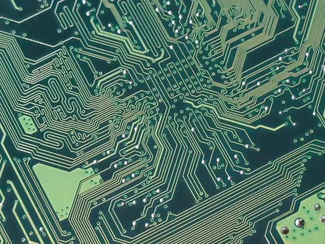
PCB hole copper inequality causes thick and thin what reason be
by:Rocket PCB
2020-06-12
Q: PCB hole copper inequality causes thick and thin what reason be?
Uneven electroplating (
UNEVENPLATING)
What are the reasons (
By using the pulse plating)
吗?
How to improve?
Current size to go with the thickness of the plating and line width have a relationship?
How the relationship?
A: I wonder if you plating equipment is to use single or bilateral control rectifier is designed, if it is single rectifier control structure, electroplating current distribution will directly affected by the contact resistance significantly.
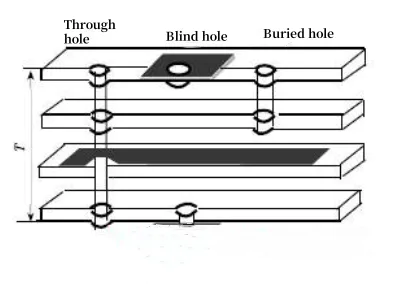
If add hole deeper and liquid flow uniformity is not ideal, the unilateral hole thickness problem is produced.
Also don't know your discussion of the circuit is the full plate electroplating or plating, if can only say that uneven plating them is inevitable, the difference is that in competitive range can do levels.
Pulse electroplating belongs to ac type electroplating, sensitivity to waveform is higher, if the contact condition is not ideal, is also likely to happen around half the of the inequality problem.
Double module PCB plating uniformity is divided into large area and small area uneven electroplating, uneven of large area, improve the probability is higher, but to improve local area was more difficult.
Generally discusses the issue of uneven plating, the main ginger concerns mainly on the distribution of the power line.
A power line for electroplating, is imaginary path of charged particles.
Factors that affect these hypothetical routes include: anode configuration mode, the polar distance of Yin and Yang, circuit boards, hang, swing yao fluid mixing, circuit boards, current density high, burnish system type, cover design, etc.
For large area, these factors can help make adjustments, but for small area especially line electroplating, because of the copper surface distribution is irregular, and configuration and design of cathode is fixed, thus inevitably produce mutually exclusive power distribution inequality phenomenon.
More efficient way at present, most of them adopt a lower current density and appropriate system to improve gloss, other mechanical design please equipment dealer adjustments should also improve space.
Current size and the plating area, we call the current density.
Current distribution more uniform, plating quality is good, and the higher the current density at the same time of copper plating thickness is short.
But often accompanied by high current density electric evenness variation problem, how to achieve a balance between the capacity and quality is the problem you have to think about.
In general, if the line is thinner, copper surface distribution, then theoretically represents the lower current density is available now.
Early circuit board manufacturers in the face of electroplating uniformity problem, there is another more direct thinking is to polar distance of Yin and Yang, this treatment can be powerline repellence to lower levels, for plating thickness uniformity is really helpful.
This kind of deal with more energy, however, is not appropriate for pulse electroplating processing method.
For line plating, dense lines area will bear more uniform current, but in a separate line area (
Uneven density area)
Current distribution will be more bad, at this time if possible should increase some false points on the circuit board to dispersed electric current, or electroplating evenness is bound to become more bad, the above information is Rocket PCB production are for reference only.
Rocket PCB as a professional supplier of PCB circuit boards, focus on high-precision double-sided/multilayer circuit board production, advanced HDI board, circuit boards, blind hole buried thick copper PCB proofing and small batch, high frequency circuit boards and PCB board production.
Under the same cost we faster delivery, under the same delivery speed our costs are lower.
At present, the Rocket PCB circuit has PCB circuit board production base and technology research and development base, in the domestic several major electronic product design center layout service center, has for more than 2000 customers worldwide rapid electronic manufacturing services.
It isn't just about being on pcb making service anymore–it's about maximizing the potential of the platform of manufacturing.
Rocket PCB Solution Ltd. will be known for our leadership edge, through our passion for high standards, our respect for diversity and our commitment to create exceptional opportunities for professional growth so that associates can fulfill their highest potential.
pcb making service is attracting a great positive feedback from the customers. And many of our clients are fully satisfied with it.
Rocket PCB Solution Ltd. constantly discovers the demands of global market for developing a wide range of products applied in different use.
Rocket PCB Solution Ltd. sells pcb manufacturing services and yet their focus on operational excellence and mastery of distributed manufacturing facilities pcb manufacturing services has made them the dominant player in the space.
Custom message
Related Products