Analysis and Countermeasures of Power Supply Noise in High-Frequency PCB Design
With the increase of the operating frequency of electronic products, there are more and more high-frequency PCB designs, but compared with low-frequency PCB designs, there are many interferences. In summary, there are four main aspects of power supply noise, transmission line interference, coupling, and electromagnetic interference (EMI). The interference of power supply noise has a far-reaching impact on high-frequency PCB design.
Distributed noise caused by the inherent impedance of the power supply itself. In high-frequency circuits, power supply noise is one of the factors that have a greater impact on high-frequency signals. Therefore, a low-noise power supply is required first. Clean ground and clean power supply are equally important.
Common-mode field interference: refers to the noise between power supply and ground. It is caused by the common-mode voltage caused by the loop formed by the interfered circuit and the common reference plane of a certain power supply. The value depends on the relative strength of the electric field and the magnetic field.
In high-frequency PCB boards, one of the more important types of interference is power supply noise. The author systematically analyzes the characteristics and causes of power supply noise on high-frequency PCB boards, and combines engineering applications to propose some very effective and simple solutions.
1. Analysis of power supply noise
1) Distributed noise caused by the inherent impedance of the power supply itself. In high-frequency circuits, power supply noise has a greater impact on high-frequency signals. Therefore, a low-noise power supply is required first. A clean ground and a clean power supply are equally important.
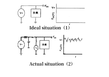
The power supply characteristics are shown in Figure 1.

Figure 1: Power supply waveform
As can be seen from Figure 1, the ideal power supply has no impedance, so there is no noise. However, the actual power supply has a certain impedance, and the impedance is distributed throughout the power supply, so the noise will also be superimposed on the power supply. Therefore, the impedance of the power supply should be reduced as much as possible, and it is best to have a dedicated power layer and ground layer. In high-frequency circuit design, it is generally better to design the power supply in the form of a layer than in the form of a bus, so that the loop can always follow the path with the least impedance. In addition, the power board must also provide a signal loop for all signals generated and received on the PCB, so that the signal loop can be minimized, thereby reducing noise.
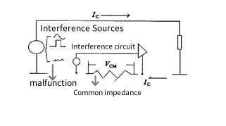
2) Common mode field interference. Refers to the noise between the power supply and the ground. It is caused by the common mode voltage caused by the loop formed by the interfered circuit and the common reference plane of a certain power supply. Its value depends on the relative strength of the electric field and the magnetic field. As shown in Figure 2.

Figure 2: Common-mode field interference
On this channel, the drop in Ic will cause a common-mode voltage in the series current loop, affecting the receiving part. If the magnetic field is dominant, the value of the common-mode voltage generated in the series ground loop is:
![]()
ΔB in formula (1) is the change in magnetic induction intensity, Wb/m2; S is the area, m2.
If it is an electromagnetic field, when its electric field value is known, its induced voltage is
![]()
Formula (2) is generally applicable to L=150/F or less, where F is the electromagnetic wave frequency in MHz.
The author's experience is that if this limit is exceeded, the calculation of the maximum induced voltage can be simplified to
![]()
3) Differential mode field interference. Refers to the interference between the power supply and the input and output power lines. In actual PCB design, the author found that it accounts for a very small proportion of the power supply noise, so it can be ignored here.
4) Inter-line interference. Refers to the interference between power lines. When there is mutual capacitance C and mutual inductance M1-2 between two different parallel circuits, if there is voltage VC and current IC in the interference source circuit, the interfered circuit will appear:
a. The voltage coupled through capacitive impedance is
![]()
In formula (4), RV is the parallel value of the near-end resistance and the far-end resistance of the interfered circuit.
b. Series resistance through inductive coupling
![]()
If there is common mode noise in the interference source, the line interference generally manifests itself in two forms: common mode and differential mode.
5) Power line coupling. It refers to the phenomenon that after the AC or DC power line is subjected to electromagnetic interference, the power line transmits these interferences to other devices. This is the indirect interference of power supply noise to high-frequency circuits. It should be noted that the noise of the power supply is not necessarily generated by itself, but may also be noise induced by external interference, and then this noise is superimposed on the noise generated by itself (radiation or conduction) to interfere with other circuits or devices.
2. How to eliminate power supply noise interference
According to the different manifestations and causes of power supply noise interference analyzed above, the conditions for its occurrence can be destroyed in a targeted manner, which can effectively suppress the interference of power supply noise. The solutions are:
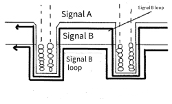
1) Pay attention to the through holes on the board. Through holes require the power layer to be etched to leave space for the through holes to pass through. If the opening of the power layer is too large, it will inevitably affect the signal loop, the signal is forced to detour, the loop area increases, and the noise increases. At the same time, if some signal lines are concentrated near the opening and share this loop, the common impedance will cause crosstalk. See Figure 3.

Figure 3: Common path for bypassing signal loops
2) The connection line needs enough ground wires. Each signal needs to have its own dedicated signal loop, and the loop area of the signal and loop should be as small as possible, that is, the signal and loop should be parallel.
3) Place a power supply noise filter. It can effectively suppress the noise inside the power supply and improve the anti-interference and safety of the system. And it is a bidirectional RF filter, which can filter out the noise interference introduced from the power line (to prevent interference from other devices) and the noise generated by itself (to avoid interference with other devices), and has a suppressive effect on series mode and common mode interference.
4) Power supply isolation transformer. Separate the common mode ground loop of the power supply loop or signal cable, which can effectively isolate the common mode loop current generated in the high frequency.
5) Power supply regulator. Regaining a cleaner power supply can greatly reduce the power supply noise.
6) Wiring. The input and output lines of the power supply should be avoided on the edge of the dielectric board, otherwise it is easy to generate radiation and interfere with other circuits or equipment.
7) Analog and digital power supplies should be separated. High-frequency devices are generally very sensitive to digital noise, so the two should be separated and connected together at the entrance of the power supply. If the signal needs to cross the analog and digital parts, a loop can be placed at the signal crossing point to reduce the loop area. As shown in Figure 4.
8) Avoid overlapping of separate power supplies on different layers. Try to stagger them, otherwise the power supply noise can easily couple through parasitic capacitance.
9) Isolate sensitive components. Some components such as phase-locked loops (PLLs) are very sensitive to power supply noise, so they should be kept as far away from the power supply as possible.
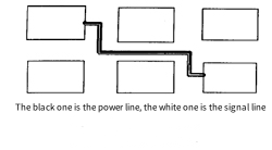
10) Place power lines. In order to reduce the signal loop, the noise can be reduced by placing the power line next to the signal line, as shown in Figure 5.

Figure 5: Placing power lines next to signal lines
11) In order to prevent the power supply noise from interfering with the circuit board and the accumulated noise caused by external interference with the power supply, a bypass capacitor can be connected to the ground on the interference path (except radiation). This can bypass the noise to the ground to avoid interfering with other equipment and devices.
Conclusion
In high-frequency circuits, the noise contained in the power supply signal has the greatest impact on high-frequency signals. All electronic signals are transmitted by the rise and fall of the level. If the secondary Jiebai power supply is superimposed with high noise, the power supply of the entire system will be unclean, and the fluctuation will cause the high-frequency signal to be distorted. Of course, it does not mean that a low-noise power supply will not affect the operation of high-frequency PCBs.
At this time, clean GND and VCC are equally important, so we need to minimize the power supply impedance as much as possible during design, and use a dedicated GND layer and VCC layer. In high-frequency circuits, designing the power supply in the form of layers will have better performance than bus design. In this way, the current loop will follow the path with the least impedance. This design can minimize the signal loop, thereby achieving the purpose of reducing noise, which is often overlooked by low-frequency circuit designers.
Power supply noise is directly or indirectly generated from the power supply and interferes with the circuit. When suppressing its influence on the circuit, a general principle should be followed, that is: on the one hand, the influence of power supply noise on the circuit should be prevented as much as possible, and on the other hand, the influence of the outside world or circuit on the power supply should be minimized as much as possible to avoid worsening the power supply noise.


