


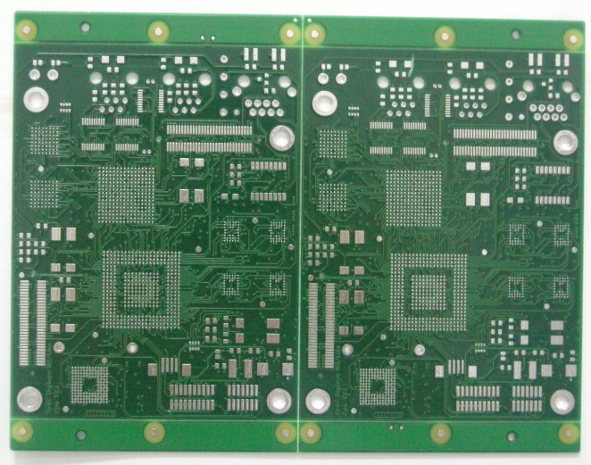
Why special treatment of PCB surface?
Because copper is easy to oxidize in air, the oxide layer of copper has a great influence on soldering. It is easy to form false welding and false welding. In serious cases, it will cause the pad and components cannot be welded. Therefore, PCB will have a process in manufacturing, coating (plating) on the pad surface to protect the pad from being oxidized.
At present, the surface treatment processes of domestic PCB manufacturers include: HASL (hot air solder leveling), immersion tin, immersion silver, OSP (anti-oxidation), immersion gold (ENIG), electroplating gold and so on. Of course, there will be some special PCB surface treatment processes in special applications.
Comparing different PCB surface treatment processes, their cost is different, of course, the occasions used are different, choose only the right one but not the expensive one. There is no perfect PCB surface treatment process (Here is the cost-effective, that is, to meet all PCB application scenarios at the lowest price), so there will be so many surface treatments to let us choose, of course, each process has its own merits, the key is to use them well.
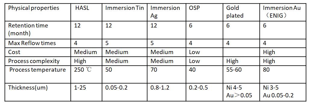
HASL, Hot Air Solder Leveling
Advantages: Low price, good soldering performance.
Disadvantage: It is not suitable for soldering pins with fine clearance and too small components, because the surface of HASL is not smooth. Solder bead is easy to be produced in PCB processing, and short circuit is easy to be caused for fine pitch components.
HASL process used to play a leading role in PCB surface treatment process. In the 1980s, more than three quarters of PCBs used HASL technology, but the industry has been reducing the use of HASL technology in the past decade. It is estimated that about 25-40% of PCBs now use HASL technology. HASL process is dirty, smelly and dangerous, so it has never been a lovely process, but HASL process is an excellent process for larger size components and larger spacing wires. In PCB with high density, the flatness of HASL process will affect the subsequent assembly, therefore, HASL process is generally not used in HDI board. At present, some factories adopt OSP process and immersion gold process instead of HASL process, the development of technology also makes some factories adopt immersion tin and immersion silver process. In addition to the trend of lead-free in recent years, the use of HASL process is further restricted. At present, lead-free HASL is more widely used.
OSP(Organic Soldering Preservative)
Advantages: With all the advantages of bare copper plate welding, the expired boards can also be re-surface treated, but usually only once.
Disadvantage: susceptible to acid and humidity. When used in secondary reflow welding, it needs to be completed in a certain time. Usually, the effect of the second reflow welding is poor. If the storage time exceeds three months, it must be re-surface treated. It should be used up within 24 hours after opening the package. OSP is an insulating layer, so the test point must be printed with solder paste to remove the original OSP layer in order to contact the needle point for electrical testing.
It is estimated that about 25% to 30% of PCBs currently use OSP technology, which has been increasing. OSP technology can be used in low-tech PCB, high-tech PCB, such as single-sided television PCB, high-density chip packaging board. For BGA, OSP application is also more. If PCB does not have the functional requirements of surface bonding or the limitation of storage time, OSP process will be the most ideal surface treatment process.
ENIG,Electroless Nickel Immersion Gold
Advantages: not easy to oxidize, can be stored for a long time, flat surface, suitable for welding fine gap pins and components with smaller solder joints. Preferred PCB board with buttons
Repeated reflow soldering also does not reduce solderability. It can be used as the base material of COB (Chip On Board)
Disadvantages: high cost, poor welding strength, because the use of non-electroplated nickel process, easy to have black disk problems. The nickel layer oxidizes over time, and long-term reliability is a problem.
Unlike OSP process, immersion gold process is mainly used on boards with connection functional requirements and long storage period, such as mobile phone keypad area, edge connection area of router shell and electrical contact area of chip processor elastic connection. Immersion Gold was widely used in the 1990s. Later, due to the emergence of black disk and brittle Ni-P alloy, the application of immersion gold process was reduced. Considering that the solder joints would become brittle when copper-tin intermetallic compounds were removed, many problems would arise at relatively brittle Ni-Sn intermetallic compounds. Therefore, almost all portable electronic products (such as mobile phones) adopt copper-tin intermetallic compound solder joints formed by OSP, silver or tin deposition, while immersion gold is used to form key area, contact area and EMI shielding area, namely the so-called selective immersion gold process. It is estimated that about 10% - 20% of PCBs currently use Electroless Nickel Immersion Gold process.
Immersion Silver
Silver is cheaper than gold. Silver is a good choice if PCB has connection functional requirements and needs to reduce costs. With good flatness and contact, Immersion Silver process should be chosen. Silver is widely used in communication products, automobiles, computer peripherals, and in high-speed signal design. Silver can also be used in high frequency signals because of its excellent electrical properties that other surface treatments cannot match. EMS enterprise recommends silver precipitation because it is easy to assemble and has good checkability. It is estimated that about 10% - 15% of PCBs currently use immersion silver process.
Immersion Tin
The appearance of immersion Tin process is the result of the requirement of production automation. No new elements are brought into the solder, especially for the backplane PCB of communication. Tin will lose solderability beyond the shelf life, so immersion tin requires better storage conditions. In addition, immersion tin process is restricted because it contains carcinogens. It is estimated that about 5% - 10% of PCBs currently use immersion tin process.
Preservation Period and Notice of PCB Surface Treatment
1. Considering the difference of process and storage conditions, PCB should be used in time (recommended within 24 hours) after disassembly, and pre-drying treatment is recommended before use, especially for PI substrate in flexible circuit board. If patch welding is needed, pre-drying treatment is necessary.
2. For immersion tin or immersion silver products, it is recommended that they be used up within 12 hours after unpacking, otherwise they must be repackaged.
3. If the shelf life exceeds the valid life, the user can try it after drying treatment: if necessary, some properties will be re-tested and can still be used after passing the test.
4. Usually, if the storage time is more than 3 months, in order to avoid dampness, it is necessary to bake for 2 hours and 150 degrees before putting the parts on the SMT machine.
Storage environment
A. Good storage conditions: refers to indoor environmental conditions with temperature control and non-corrosive gases, where the temperature is less than 25 degrees and the relative humidity is less than 65%.
B. General storage conditions: refers to indoor environmental conditions in which the temperature is not higher than 35 degrees, the relative humidity is not more than 75%, and corrosive gases are not present.


