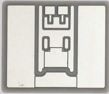
The guide hole (
VIA)
Between different layers of conductive graphics, circuit board copper foil line is to use the hole conduction or connected, but not instrumentation component lead leg or other reinforced material of copper plated holes.
Printed circuit board (
PCB)
Is formed by many of the copper foil layer stack accumulate.
Copper foil layer between each other can't each other because each layer of copper foil were covered with a layer of insulation, so they need to rely on conduction between hole (
via)
To signal link, so there will be a Chinese guide hole.
Circuit board guide hole plug hole must be made to meet customer demand, to change the traditional process of aluminium plug hole, PCB board face resistance welding and jack use white mesh is complete, make the production more stable, more reliable quality, more perfect.
Guide hole help circuit connected conduction, with the rapid development of electronic industry, but also on the
printed circuit board (
PCB)
Production process and surface-mount technology put forward higher requirements.
Blind buried orifice (
Printed circuit board)
PCB PCB of guide hole plug hole technology arises at the historic moment, simultaneously must satisfy the following requirements: 1.
PCB hole with copper, resistance welding can plug can not plug;
2.
Circuit board guide hole must have solder resist ink plug hole, not pervious to light, can not have tin and tin beads, must be flat and other requirements;
3.
PCB hole must be tin lead, has the certain thickness requirements (
4um)
To avoid solder resist ink into the hole, hole Tibetan beads.
Blind hole circuit board, is the printed circuit board (
PCB)
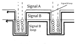
Between the outermost layers of the lining of the circuit and the adjacent to connect with plating hole, unable to see the opposite, so called blind.
In order to increase the space utilization rate between board circuit layer, blind hole will come in handy.
Blind hole, that is, to a guide hole on the surface of the PCB.
Blind hole located at the top of the circuit board and the underlying surface, have a certain depth, used for surface line with inner layer below line connection, the ratio of the depth of the hole generally has a regulation,
The aperture)
。
This way of production need to pay special attention to, drilling depth must be just right, do not pay attention to words will cause hole plating hard.
So few factories will use this way.
Actually gives in advance connected to circuit layer in the individual circuit when the first drill hole, and then sticking up also can, but need more precision positioning and contrapuntal device.
Is buried hole circuit board, printed circuit board (
PCB)
The connection between internal any circuit layer, but with no outer conduction, that no extension to the guide hole on the surface of the circuit board.
In the circuit board factory production process by bonded before drilling of circuit board, must be in the individual circuit layer when drilling operation, after the local bonding lining to the plating processing, finally all bonding.
Due to the operation process than the original guide hole and blind hole is more difficult, so the price is also the most expensive.
This process usually used only for high density circuit board, increase the space utilization of other circuit layer.
In the printed circuit board (
PCB)
In the production process, the drilling is very important.
Drilling is simple understanding on copper clad needed to drill a hole, has to provide electrical connections, fixed function of the device.
If the operation is not correct lead to problems via process, the device cannot be fixed on the circuit board, light affect the use of the circuit board, or let the whole board scrap, so the drilling process is quite important.
Rocket PCB Solution Ltd. have now make a decision to enlarge our company in other countries.
Compare the various types of that are available. At Rocket PCB , the range is constantly being updated with new models, technical details and competitive prices.
Choose the right platform for selling pcb making service and we'll reach the right customers. But if we have the right idea in the wrong platform, that still adds up to the wrong idea.
Rocket PCB Solution Ltd. provides a way for you to understand your customers, to learn what makes them unique and what motivates their behavior. We can then leverage that wealth of information to personalize our interactions and demonstrate that pcb making service is valuable to our customers.