


IC substrate is the core material of the packaging link and has a high technical threshold. IC substrate directly loads the chip, provides an electronic connection between the chip and the PCB motherboard, plays the role of "connecting the above and the next", and is a necessary core material in IC packaging technology. With the development of semiconductor technology, the characteristic size of IC continues to shrink, and the integration continues to improve. The corresponding IC package towards super multi-pin, narrow pitch, ultra-miniaturization direction in high-level packaging, IC substrate has replaced the traditional lead frame, becoming an indispensable part of the IC package.
Due to the small size of the IC substrate products, high precision, higher requirements in line fine, hole distance size and signal interference, more accurate interlayer alignment technology, electroplating capacity, and drilling technology in manufacturing. The process flow of IC substrate is complex, involving many processes, and it takes a long time to accumulate experience to optimize the appropriate parameters. This article will lead you to a comprehensive understanding of IC substrates, introduce the development and manufacturing process of IC substrates, as well as market development trends and manufacturers.
What is the IC substrate in the Semiconductor package?
The IC substrate is the key component in the IC package. The substrate connects and transmits the signal between the bare chip (DIE) and the printed circuit board (PCB). The upper layer of the package substrate is connected to the chip, and the lower layer is connected to the printed circuit board to achieve electrical and physical connection, power distribution, signal distribution, and communication between the chip's internal and external circuit functions.
As the core material of the chip package, the package substrate can protect, fix, and support the chip, enhance the thermal conductivity of the chip, and ensure that the chip is not physically damaged.

IC substrate, also known as IC package substrate, is developed based on HDI board and is adapted to the rapid development of electronic packaging technology innovation, with high density, high precision, high performance, miniaturization, and thin and other excellent characteristics. A complete chip comprises a bare chip (wafer) and a package body (package substrate, solid sealing materials, leads, etc.).
The development road map of the IC substrate
IC substrate is used in the integrated circuit packaging stage. With semiconductor technology's development, IC substrates' feature size continues to shrink. With continuous integration improvement, the corresponding IC packages are developing in ultra-multi-pin, narrow pitch, and ultra-miniaturization. So far, the global integrated circuit packaging technology has undergone five stages of development.
At present, the mainstream technology of the global packaging industry is in the third stage based on CSP BGA and is moving to system-level packaging (SiP). And the fourth and fifth stage packaging technology, represented by Flip-chip packaging (FC) and on-chip Bumping, is moving forward.
Taking 2000 as the node, the packaging industry is divided into the traditional and advanced packaging stages.
The first stage: was before the 1970s (DIP original era). The main packaging technology is pin insertion (PTH), and the main form is CDIP.PDIP. And transistor package (T0). Because it is difficult to increase the density and frequency, it is not enough to automate production requirements.
The second stage is the mid-1980s (surface mount era). From the pin insertion package to the surface patch package, the assembly density of the printed circuit board has been greatly improved, and it is easy to produce automatically. Still, the performance is poor regarding package density, 1/0 number, and circuit frequency, which is difficult to meet the development needs of ASIC and microprocessors.
The third stage: The 1990s entered the era of area array packaging. The main packaging forms are BGA, CSP, and WLP. BGA technology shortens the connection distance between the chip and the system and keeps the chip packaging technology up with the chip development pace. CSP technology solves the long-standing fundamental contradiction that the chip is small and the package is big, triggering a revolution in integrated circuit packaging technology.
The fourth stage: at the end of the 20th century, it entered the era of microelectronics packaging technology stacked packaging, which evolved from the original concept of packaging components into packaging systems. Typical packaging situations include MCM, and 3D. SIP, Bumping.
The fifth stage: Starting from the first decade of the 21st century, the typical packaging situation is system-level single-chip packaging (SoC). Microelectromechanical system package (MEMS).

Currently, advanced technology IC substrates include:
CSP (Chip-level Package)
FC-CSP (Flip chip) CSP
BOC (chip on board)
PoP (Laminated package)
PiP (package within a package)
SiP (System Level Package)
Rf module
LED package
What's the IC substrate material
Currently, there are three kinds of hard packaging substrate materials: BT, ABF, and MIS. Flexible substrate includes PI (polyimide) and PE (polyester) resins, and ceramic substrate materials mainly include alumina, aluminum nitride, silicon carbide, and other ceramic materials. The rigid and flexible substrate has more room for development, while the co-fired ceramic substrate tends to slow down.
BT substrate is a kind of resin material developed by Mitsubishi Gas; good heat resistance and electrical properties make it replace the traditional ceramic substrate; it is not easy to heat and shrink, is stable in size, is a hard material, thick line, and is mainly used for mobile MEMS, communication and storage chip packaging.
ABF substrate is an increased-layer film material developed by Ajinomoto Japan, with higher hardness, thin thickness, and good insulation. It is suitable for IC packaging of fine line, high-level number, multi-pin and high information
transmission and is used in high-performance CPU, GPU, chipsets, and other fields. Ajinomoto completely monopolizes the production capacity of ABF, and it is the key raw material for domestic IC substrate production.
MIS is a new type of material, different from the traditional substrate, consisting of one or more layers of pre-packaged structure; each layer is interconnected by electroplating copper, thinner line, better electrical performance, smaller volume, and rapid development in the field of power, analog IC and digital currency.
The main considerations for selecting IC substrate materials include dimensional stability, high-frequency characteristics, heat resistance, and thermal conductivity.
A variety of classification ways for IC substrates
Synthesizing the above substrate material description can also be seen that the type of packaging substrate according to different materials, technologies, and processes produced by the IC substrate properties are different, and the final scope of application is different. The mainstream classification of the packaging substrate is through the substrate material, packaging process, and application field.

According to package technology
According to the mainstream package, IC substrate can be divided into WB-BGA, WB-CSP, FC-BGA, FC-CSP, and other four categories; FC-BGA technology requirements are the highest.

WB and FC
Wire bonding (WB) uses fine metal wire. It uses heat, pressure, and ultrasonic energy to tightly weld the metal lead, chip pad, and substrate pad to realize the electrical interconnection and information interworking between the chip and substrate. It is widely used in RF modules, Memory chips, and MEMS device packages.
Flip-Chip (FC) is different from wire bonding; it uses a welding ball to connect the chip and the substrate; that is, the welding ball is formed on the chip pad, and then the chip is flipped and pasted on the corresponding substrate, and the chip and the substrate pad are combined by heating and melting the welding ball. This packaging process has been widely used in CPU and GPU.
FC, due to the use of tin ball instead of lead, compared with WB to improve the substrate signal density, improve chip performance, convex point alignment correction is convenient, improve yield, is a more advanced connection.

BGA and CSP
BGA/CSP is the connection between the IC substrate and PCB; CSP is suitable for mobile chips, and BGA is suitable for PC/server-level high-performance processors. BGA (Ball Grid Array) is arranged at the bottom of the chip in an array of tin balls, with the tin ball array instead of the traditional metal wire rack as the pin.
CSP (Chip Scale Package) can make the ratio of chip area to package area more than 1:1.14, which is quite close to the ideal situation of 1:1, about 1/3 of the ordinary BGA, which can be understood as the BGA with smaller tin ball spacing and diameter. From the downstream application point of view, FC-CSP is mostly used for mobile devices AP, baseband chip, FC-BGA is used for PC, server level CPU, GPU and other high-performance chip packaging substrate with many layers, large area, high line density, line width and line distance small through the hole, blind hole aperture and other characteristics, its processing difficulty is much greater than FC-CSP packaging substrate.
Chart1. Different IC substrate package technologies Comparision
According to the bonding mode | Type | Product application field | End products | ||
WB | BGA | Ball Grid Array |  | Microprocessor, Southbridge chip, networking chip | Tablets, laptops, phones, game consoles, etc |
CSP | Chip Scale Package |  | Computer memory, cell phone, flash memorycard | Computer, cell phone, camera, video camera. | |
RF Module |  | Rf power amplifier, transceiver, front-end receiver module | Cell phones, tablets, game consoles, computers, etc | ||
Digital Module |  | Digital camera memory card | Digital camera | ||
FC | FC BGA |  | Microprocessor, graphics processor, baseband chip, application processor, game console processor, | Computers, tablets, game consoles, etc | |
FC PGA | FC Pin Grid Array |  | Microprocessor | Computers, tablets, game consoles, etc | |
FC LGA | FC Land Grid Array |  | Microprocessor | Computers, tablets, game consoles, etc | |
FC CSP |  | Application processor, baseband chip, smartphone, acceleration processor, power management, power line | Cell phones, tablets, cameras, camcorders, digital TV |
According to the material of the IC substrate
As mentioned above, IC substrate materials contain several categories as shown in the figure below.
Chart2. Different IC subtrate package technologies Comparision
Substrate classification | Substrate material | Features | Main application fields |
Rigid IC substrate | BT | high Tg (255-330℃), high heat resistance (160-230℃), moisture resistance, low dielectric constant (DK) and low loss factor (DF), but it can not meet the requirements of thin line | MEMS, communication, memory chips, and LED chips |
ABF | High hardness, thin thickness, good insulation, can be made large size, Fine-line, high-number, multi-pin, high-information transmission IC package | It is mainly used for large high-end chips such as CPU, GPU and chipset | |
MIS | Different from the traditional substrate, it contains one or more layers of pre-encapsulated structure, each layer is interconnected by electroplating copper to provide an electrical connection in the packaging process. | It has developed rapidly in analog, power IC and digital currency markets | |
Flexible IC substrate | PI | It is mainly divided into three-layer glued substrate and two-layer non glued substrate, with excellent heat resistance, good moisture absorption and mechanical properties | It can be used in carrier rocket, cruise missile, space satellite and other military chips, as well as automotive electronics, consumer electronics and other chips |
PE | |||
Ceramic IC substrate | Alumina | Ceramics are inorganic insulating materials, which have the advantages of heat resistance, thermal stability and high-frequency characteristics, but the machinability is poor and the cost is high | It is mainly used in thick film circuit, thin-film circuit and military chip |
Aluminum nitride | |||
Silicon carbide |
According to the IC substrate application
From the final application point of view, according to the different types of IC finished products, the packaging substrate (IC substrate) can be divided into memory chip packaging substrate, MEMS packaging substrate, RF module packaging substrate, processor chip packaging substrate, and high-speed communication packaging substrate. Memory chip packaging substrate is mainly used for smartphone and tablet computer storage modules and solid state disks; Mems packaging substrate is mainly used for sensors of smartphones, tablets, and wearable electronic products; Rf module packaging substrate is mainly used for RF module of mobile communication products such as smartphones; The processor chip packaging substrate is mainly used for the baseband and application processor of smartphones, tablet computers, etc.
Chart3. IC substrate (package substrate) is classified by application field
| Product name | Product display | Application |
| eMMC IC substrate | 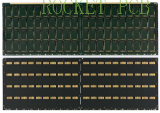 | Smart phone and tablet storage modules, solid state drives, etc |
| MEMS IC substrate | 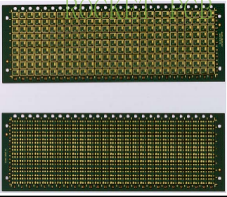 | Sensors for cell phones, tablets, wearable electronics, etc |
| RF module IC substrate | 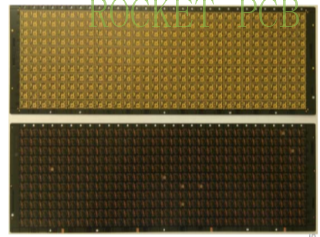 | Rf modules for mobile communication products such as smartphones |
| WB-CSP IC substrate | 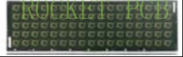 | Baseband and application processor for mobile phones, tablets, etc |
| FC-CSP IC substrate |  | Baseband and application processor for mobile phones, tablets, etc |
| High-Speed communication IC substrate |  | Data broadband, telecommunication communication, FTTX, data center, security monitoring and smart grid conversion modules |
IC substrate vs PCB
IC substrate performance is excellent, and the application proportion continues to increase. Compared with the conventional PCB board, the package substrate line width and line distance are smaller, and the board size is smaller, which can meet the strict requirements of the mainstream chip. Line width/line distance 50um/50um belongs to the high-end products of PCB, and in the field of packaging substrate manufacturing, line width/line distance within 30um/30um belongs to the conventional products.
With the development of technology towards high density and high precision, the proportion of high-end product packaging substrate in PCB board is also gradually increased. According to Prismark, the packaging substrate accounted for 8.43% of the PCB board in 2000, the packaging substrate accounted for 15.68% in 2020, and it is predicted that by 2026, the packaging substrate will account for 21.11%, accounting for a steady increase.
Chart4. IC substrate, SLP, HDI and ordinary PCB parameter comparison
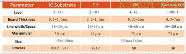
Compared to traditional PCB technology, IC substrates are more difficult and have higher entry barriers.
The technical threshold of the IC substrate is high. IC substrate has the characteristics of high density, high foot number, high performance, miniaturization and thinness, and its technical parameters are much higher than HDI and ordinary PCB. IC substrate for line width/line distance parameters requirements in 10-30um, and ordinary PCB line width/line distance is more than 10um. Has entered the semiconductor process, PCB technology development path is from multi-layer PCB to traditional HDI PCB, SLP and then to IC substrate, IC substrate manufacturing process and semiconductor approximate, IC substrate process is mSAP or SAP, the traditional PCB is reduced to etching process.
Compared with standard PCB products, the technical difficulties of IC substrate in manufacturing are mainly reflected in the following:
IC substrate manufacturing technology: the core board is thin and easily deformed.
Microvia technology. There are higher requirements for the hole shape, the ratio of aperture up and down, side erosion, glass fibre protrusion, and residual glue at the bottom of the hole.
Precision interlayer alignment technology, more detailed line imaging technology, and copper plating technology, and different product detection technology from traditional PCB.
Solder resistance film technology
Surface treatment technology
Inspection capability and product reliability testing techniques
Chart5. The main technical difficulties of IC substrate manufacturing
Technical classification | Problems | Difficult points |
IC substrate manufacturing | IC substrates are thin and easily deformed | Breakthroughs in substrate shrinkage, lamination parameters and lamination positioning systems are necessary to effectively control substrate warping and lamination thickness |
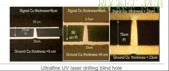
Microvias fabrication techniques | Through holes are much smaller than standard PCBS | conformal mask,laser drilling micro blind through-hole technology, and copper plating filling technology. |
Pattern and copper plating technology | The l ine width/line distance is smaller than the standard PCB, and the pattern is more fine | Circuit compensation technology and control, fine line manufacturing technology, copper plating thickness uniformity control |
Solder mask | Through hole filling technology, solder mask printing technology and other requirements are high | The surface height difference of the IC substrate is less than 10um, and the surface height difference between the solder stop layer and the pad should not exceed 15um |
Surface treatment | Surface finish should emphasize thickness uniformity | Acceptable surface finishes for IC substrate PCBS include ENIG/ENEPIG |
Inspection capability and product reliability testing techniques | Product reliability requirements are high | Different inspection equipment and operators are required from traditional PCBS |
The production process of IC substrate
There are three kinds of IC substrate manufacturing Processes, the SP (subtraction Process) , SAP (semi-additive Process) and MSAP (modified Semi Additive Process).
SAP and MSAP are used for products with line width/line spacing less than 25μm and more complex process flow. SAP and MSAP are produced similarly, briefly described as coating a thin copper layer on a substrate, followed by a graphic design, then electroplating the required thickness of the copper layer, and finally removing the seed copper layer. The basic difference between the two processes is the thickness of the seed copper layer. The SAP process starts with a thin electroless copper coating (less than 15um), while the MSAP process starts with a thin layer of laminated copper foil (greater than 15um).
Recommended reading: IC Substrate Technology Guide
Chart6. Subtraction Process flow

Chart7. MSAP flow

Chart8. The advantages and disadvantages of SP, SAP and mSAP
SP | SAP | MSAP | |
Line width | ≥75um | 10um-50um | 10um-50um |
Side erosion effects | There is a lot of side erosion | Less side erosion | Less lateral erosion |
Uniformity of coating thickness | Full plate plating, good uniformity | Pattern electroplating current distribution is not uniform, resulting in a decline in the uniformity of the pattern | Pattern electroplating current distribution is not uniform, resulting in a decline in the uniformity of the pattern |
Resin adhesion | Good | Good | The adhesion is poor, so it is necessary to coarsene the surface of the resin and improve the e’less copper process |
Thermal stress and reflux test | Meet the requirements | Meet the requirements | There is a bad risk of delamination |
Craft difficulty | General | General | General |
Degree of environmental impact | More copper consumption and more etching fluid consumption | Reduce the consumption of copper while reducing the consumption of etching fluid | Reduce the consumption of copper while reducing the consumption of etching fluid |
2023-2027 Global IC substrate market and major manufacturers
IC substrates are mainly driven by AP, FC CSP, and baseband of 5G wireless devices, HPC, GPU, server, and FC BGA in the automotive industry. Yik Yee Tan, senior technology and market analyst at Yole Intelligence, said, "The global advanced IC substrate market will grow in value from US $15.8 billion in 2021 to about US $29.6 billion in 2027, a compound annual growth rate (CAGR) of 11%. This growth is primarily driven by high demand from the mobile and consumer, automotive and mobility segments, and telecom and infrastructure markets."
According to Frost & Sullivan statistics, the market size of advanced packaging in the Chinese mainland in 2020 was 35.13 billion yuan, and it is expected to grow to 1113.66 billion yuan in 2025, with a compound annual growth rate of 26.47% from 2020 to 2025. Higher than Yole's forecast of a 9.6% compound annual growth rate of the global advanced packaging market.
The main substrate technology trends are the continued increase in complexity, larger areas, more layers, finer spacing, and the use of semi-addition processes (SAP), modified SAP (mSAP), or advanced mSAP (amSAP) to reduce line/width spacing (L/S). IC substrate vendors have been improving packaging technologies to meet their stringent requirements for smaller footprints, higher performance, and lower power consumption. Energy consumption. The demand for consumer electronics and mobile communication devices is pushing electronics manufacturers to create smaller, more portable products.
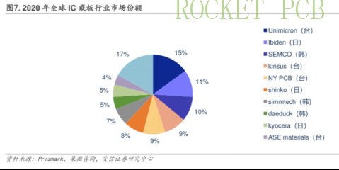
Ibiden, Unimicron, Semco, Simmtech, Kinsus are all major IC substrate producers. About 45 % of global sales are accounted for by the top five vendors. Asia-Pacific is the biggest consumer market with 87 % followed by Europe and North America. FC-BGA has the largest share in terms of type with about 30%. In terms of application, smartphones are the most popular, followed by PC (tablets, Laptops).
Chart9. 2020 Global IC substrate market share
The IC substrate market is optimistic, especially the FC BGA market of ABF IC substrate. Several companies have announced massive investments and capacity expansions of more than $15.5 billion in 2021 and 2022. More investment will occur in Asia, with nearly 46% in China. The largest investor is Austria's AT&S, which focuses on FC BGA and aims to become a top three global IC substrate supplier shortly.
The key players in the advanced IC substrate market are:
ASE Group (Taiwan)
TTM Technologies (USA)
KYOCERA Corporation (Japan)
Eastern (US)
Ibiden (Singapore)
AT&S (Austria)
Nan Ya PCB (Taiwan)
Semco (US)
Fujitsu (Japan)
Daeduck (South Korea)
Korean Circuit (South Korea)
Shinko Electric Industries (Japan)
Zhen Ding Technology (Taiwan)
Unimicron (Taiwan)
Kinsus (Taiwan)
Shenzhen Fastprint Circuit Tech (China)
Zhuhai ACCESS Semiconductor (China)
Shennan Circuit (China)
LG Innotek (South Korea)
Simmtech (South Korea)
Chart10. 2020-2021 Global ABF substrate market share (from YOLE Intelligence)
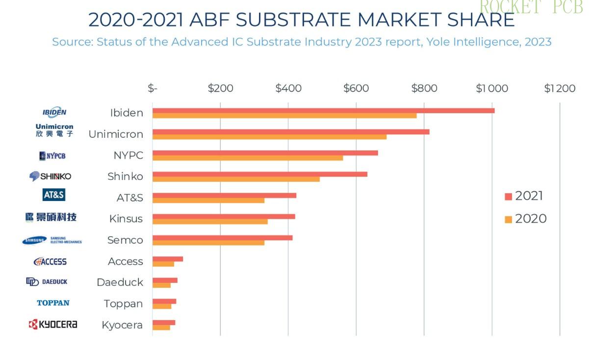
Chart11. 2021-2022 IC substrate Investment ranking (from YOLE Intelligence)
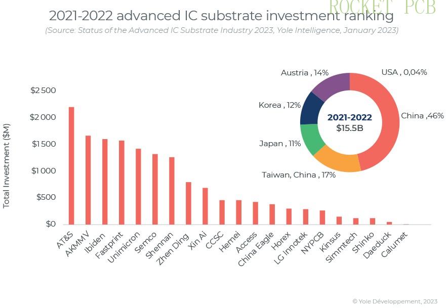
Chart12. 2021-2027 Advanced IC substrate market revenue (from YOLE Intelligence)
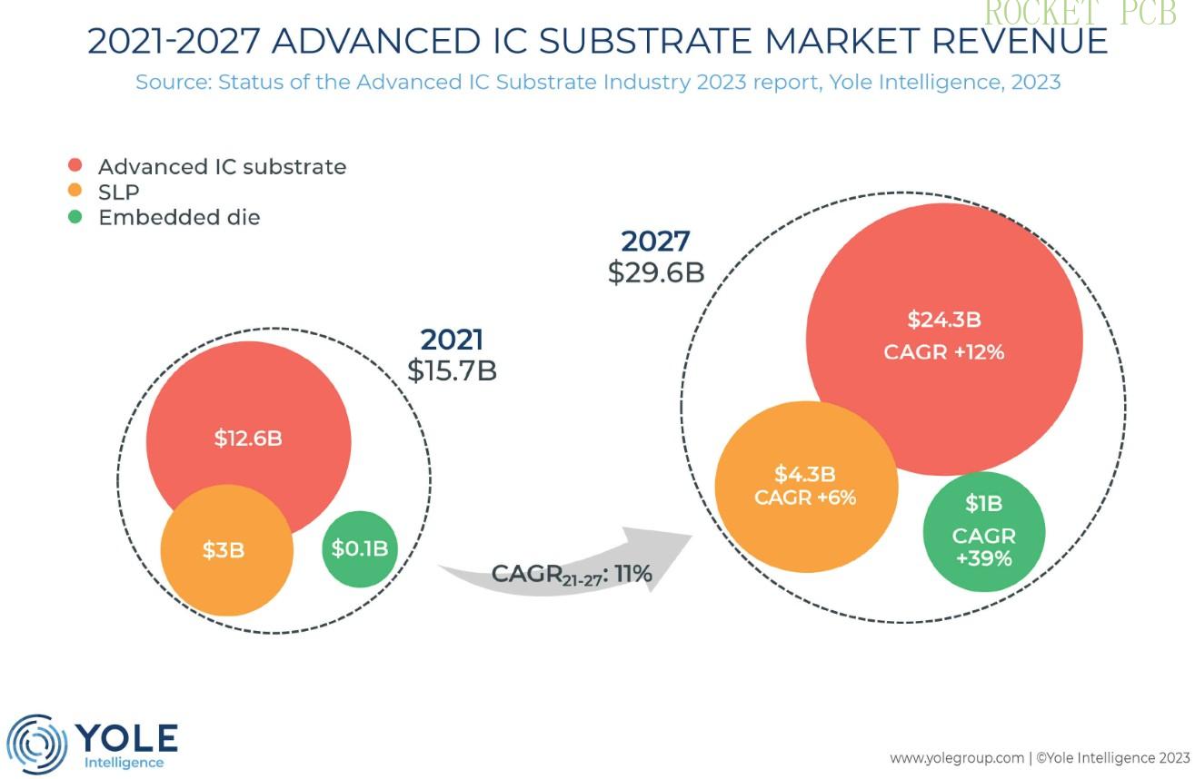
Chart13. The core product layout of the world's top 10 substrate manufacturers

From the above companies, due to the high technical barriers and capital investment of IC packaging substrate, the current global packaging substrate market is occupied by PCB enterprises in Japan, Taiwan, South Korea and other regions, the market share of the top ten enterprises exceeds 80%, and the industry concentration is relatively high.
And China's local PCB enterprises, in the early growth stage, only a few of the mainland's leading PCB enterprises began to develop and mass-produce IC packaging substrates. The Chinese mainland market is mainly dominated by three Taiwanese enterprises, an Austrian company, and three mainland enterprises: Taiwan UMTC, Kinsus, and Nanya Circuit have IC packaging substrate factories in Suzhou and Kunshan, and AT&S has IC packaging substrate projects in Chongqing. Mainland local enterprises Shennan Circuit, Fastprint Technology and Zhuhai Access have set up factories or invested in new projects in Shenzhen Longgang, Wuxi, Zhuhai and Nantong.
Chinese mainland players have a smaller market share. The localization rate is extremely low in high-end products such as ABF IC substrates. There is a huge space for Chinese manufacturers to seize the opportunity of overtaking corners.
In terms of production expansion, the main direction of the world's leading IC substrate suppliers is ABF IC substrate, while Chinese mainland suppliers are still dominated by BT IC substrate. Some PCB manufacturing companies are planning to expand the production of ABF boards. Related projects are expected to start production in 2023, with mainland Chinese manufacturers entering the high-end IC substrate market.
With the technological upgrade and application scenario expansion of products such as 5G communication, artificial intelligence, cloud computing, autonomous driving, smart wear and smart home, the demand for advanced packages such as chipsets has grown significantly. The global IC substrate industry has entered a period of rapid development.
At the same time, with the development of Chiplet, 2.5D/3D and other advanced packaging technologies, the demand area for ABF substrate has also increased significantly. The development of volume and price dual line has become an important basis for improving the ABF substrate market scale.
Conclusion
Rocket PCB is a professional and well-established manufacturer of PCBs and PCBA, offering customized services for PCB design and processing. We specialize in solving customers' research and development challenges, providing technical solutions, and delivering 24-hour service to customers worldwide. Our unique expertise in IC substrates has successfully lowered the entry threshold for customers' IC substrate production. We aim to break down barriers in IC substrate production while addressing sample/small batch production issues our customers face.


