


High Speed PCB Design
PCB layout and wiring has a key role in high-speed circuits. PCB is like a microcosm of a complete product, although the current EDA tools are very powerful, but with PCB size requirements are smaller and smaller, the device density is increasingly high, PCB design is difficult. Especially in the high-speed PCB design, engineers need to consider more issues.
1. Overview of high-speed PCB
High-speed PCB design is developed with the massive increase in system design complexity and integration, because when the system is operating at 50MHz, there will be transmission line effects and signal integrity issues. When systems operate at 120MHz, PCBs designed based on traditional methods will not work unless knowledge of high-speed circuit design is used.
2. High-speed PCB design steps
2.1. Preliminary Preparation
The information needed for PCB board design includes preparing component libraries, package libraries and schematics, and drawing mechanical dimensions in the PCB design environment based on the determined board dimensions and various mechanical positioning.
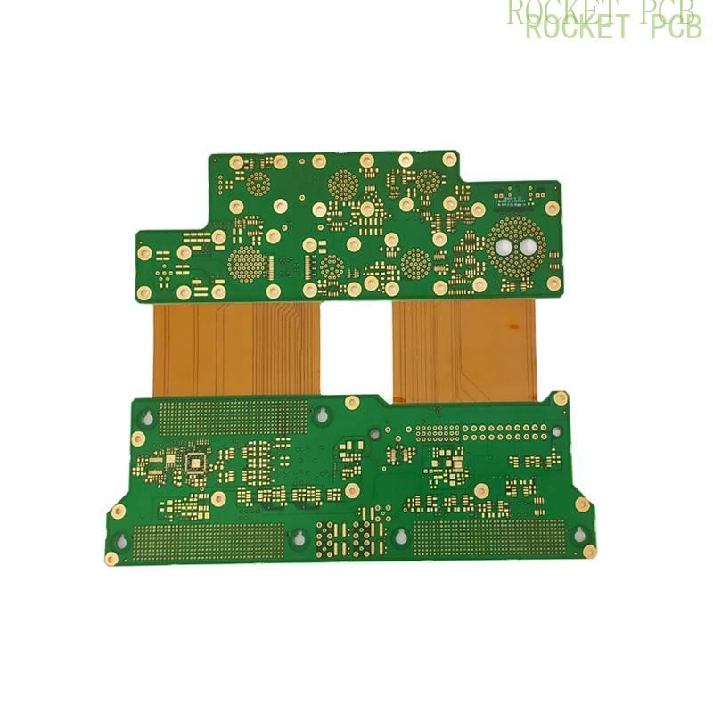
2.2. PCB Layout
When placing components, be sure to consider the actual size of components (the area and height occupied), the relative position between components to ensure the electrical performance of the board and the feasibility and convenience of production and installation at the same time, should ensure that the above principles can be reflected under the premise of appropriate modifications to the placement of devices, so that it is neat and beautiful, such as the same devices to be placed neatly, the same direction, etc.
2.3. Wiring
Cabling is the most important process in the entire PCB design. This will directly affect the performance of the PCB. Under normal conditions, power and ground lines should be wired first to ensure the electrical performance of the board. Within these conditions, try to widen the width of the electrical and ground wires. Grounding wires are better than power wires. Pre-draw the more demanding lines (such as high-frequency lines), the edges of the input and output should avoid adjacent parallel to avoid reflected interference. If needed, add grounding, and the wiring of two adjacent layers should be perpendicular to each other to prevent parasitic coupling from leading to occur.
2.4. Add teardrop
Teardrop is a drip connection between the pad and the line or between the line and the pilot hole. The purpose of setting teardrop is to avoid the contact point between the wire and pad or wire and guide hole when the board is subjected to large external forces. In addition, disconnected, the teardrop setting can make the PCB board looks better.
2.5. Design verification
After the board design is completed to check the design of the board can be taken to ensure that the PCB board is fully compliant with the requirements of the designer, and all the networks have been correctly connected, even with a wealth of experience in the design staff, the PCB board is more complex is also prone to error, so this step should not be omitted
3. High-speed pcb design considerations and solutions
3.1. Reasonable selection of the number of layers
High-frequency circuits are often highly integrated and have a high wiring density, so multilayer boards must be used. Reasonable choice of layers, can significantly reduce the printed circuit board ruler to use the middle layer to set shielding, better achieve close to ground, effectively reduce parasitic inductance, effectively shorten the signal transmission length, significantly reduce the cross-talk between signals, etc.. All of these are conducive to the reliable work of high-frequency circuit data show that the same material four-layer board to lower noise than the double-sided board, but the higher the number of layers, the more complex the manufacturing process, the higher the cost.
3.2. High-speed devices between the pins wiring
Reduce the bending of the leads between the pins of high-speed circuit devices. The leads of high-frequency circuit wiring should be straight, and if you need to bend them, you can use 45° fold lines or circular arcs, which can reduce the emission of high-frequency signals and the coupling between them. Shorten the leads between the pins of high-frequency circuit devices. The most effective means of meeting the shortest wiring is. Reduce the alternation of lead layers between the pins of high-frequency circuit devices.
3.3. Pay attention to cross-talk
Pay attention to the cross-talk introduced when the signal lines are in close parallel alignment. If parallel distribution can not be avoided, the parallel signal lines can be arranged in the opposite side of a large area of ground, thereby significantly reducing interference. Parallel alignment within the same layer can hardly be avoided, but in the adjacent 2 layers of the alignment direction must be taken as perpendicular to each other, in the high-frequency circuit wiring is best in the adjacent layers of horizontal and vertical wiring respectively. After laying copper circuit board, in addition to improving the high-frequency anti-interference ability, but also on heat dissipation, improve the strength of the printed circuit board has great benefits.
3.4. Important signal line processing
Particularly important signal lines or local units to implement ground encapsulation measures. The clock and other units of local ground wrapping processing will also be very beneficial to high-speed systems. All types of signal lines can not form loops, nor can they form current loops. A high frequency decoupling capacitor should be set near each IC block.
3.5. Ground design
When the signal operating frequency is greater than 10MHz, the ground impedance will become very large, then the ground impedance should be reduced as much as possible, should be used near the multi-point grounding method. Separate the digital circuit from the analog circuit, the ground of the two do not mix, and are connected to the ground of the power supply. To maximize the grounding area of the linear circuit. Try to thicken the ground wire If the ground wire is very thin, the ground potential will change with the change of current, resulting in unstable timing signal level of electronic equipment, anti-noise performance becomes bad. Therefore, the ground wire should be made as thick as possible so that it can pass 3 times the allowable current of the PCB. If possible, the width of the ground wire should be greater than 3mm. When designing the ground system of a PCB consisting only of digital circuits, the ground wire should be designed as a closed loop, which can significantly improve the noise immunity.
4. High-speed PCB design of EMC issues
PCB is like a microcosm of a complete product. It is the most explored part of EMC technology, is the highest frequency of the equipment, at the same time, is often the lowest level, the most sensitive part of the EMC design of the PCB, in the design has included grounding design, decoupling bypass, etc., a PCB with a good ground plane, not only to reduce the voltage drop generated by common mode current, but also an important means of reducing the loop. In the PCB wiring, enhanced EMC does not bring additional costs to the final product. If in PCB design, product designers tend to focus only on increasing density, reducing occupied space, pursuing aesthetics and uniform layout, ignoring the impact of line layout on EMC, in the end, the whole board has to be rewired. Therefore, to develop good PCB wiring habits at the beginning is the most cost effective way.
5. Conclusion
High-speed PCB design is a very complex design process, the content of this paper focuses on high-speed PCB design issues, there are several factors to be considered in the design, these factors are sometimes opposed to each other, a successful high-speed PCB design basically has to have stable performance, overall aesthetics, ease of application, reasonable cost and other characteristics, so in the design, you need to weigh all factors, to make a comprehensive compromise to meet the design requirements, but also to
reduce the complexity of the design.


