


Soft Gold Plating for PCB manufacturing
There are soft gold and hard gold when choosing the gold plating process to make PCB. This paper introduces two methods of soft gold plating pad.
Process A
Soft gold plating before making an outer pattern.
Process Overview
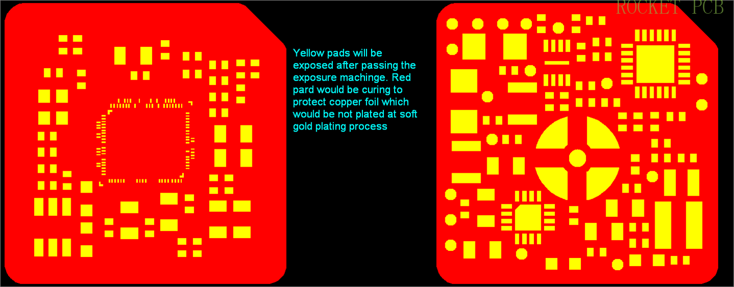
1.Use the dry film to cover all copper foil on the outer layer.
2.Pass exposure machine to make it cure. But only let the copper pads exposed.
3.Only Plate soft gold on copper pads which was exposed after the exposure process.
4.Follow standard manufacturing to do the next process, pattern transfer, and tracks etching
Disadvantage:
Copper on the side will be exposed in the gold plating area (Copper thickness direction), which has a certain impact on the reliability.
Flow Chart:
... ...--- Drilling---PTH---Full Board Plating--- Paste film,expose,develop to expose the gold-plated area---Soft Gold Plating---Etching remove the dry film--Inspection--- Other patterns--... ...
Process B
Soft gold plating after making the outer pattern and the lead wire
Overview
1. All tracks and pads would be etched out. And also make sure the electrode on the unit to connect the pads with the plating bar of the working panel.
2.And follow the solder mask layer to do the solder mask process
3.Now only pads were exposed after the solder mask process
4.Go to the next process-soft gold plating.
5.If we follow Process B, the electrode has to be left on the unit, and it will be hurt on the routing process; which means we have to accept copper exposed and burrs around the outline at the electrode area.
Flow Chart:
... ---Outer Pattern Finished--- Soldermask (Anti-Plating oil) and expose---gold plating--- remove oil---... ... ( If want to remove the lead wire, the next flow as below, --- second solder mask and expose (protect the all pattern, opening the lead wire area)---etching the lead wire--- remove the oil--- Normal solder mask---silkscreen---... ...
Disadvantage:
Very long process flow, high cost.
The local area of gold plating is prone to under corrosion or over corrosion.
The short gold-plated lead wire remains.
Bonding area
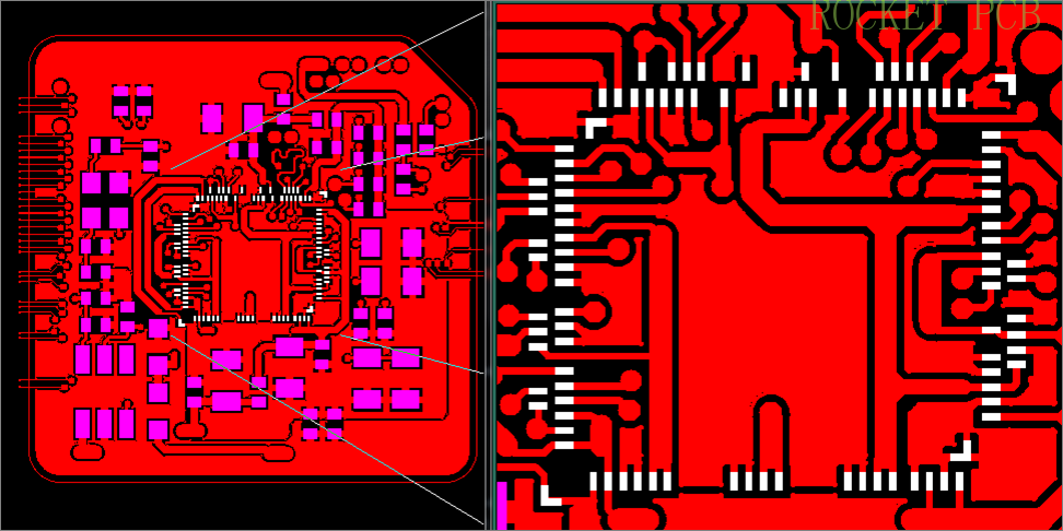
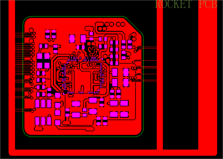
•Follow Gerber design and our manufacturing experience. We think only QFN on the top layer needs the bonding. You can see white pads shown in the picture on the next page.
•If only to do Electrolytic soft gold plating on these pads, it seems Au cost can be saved. But for this selective soft gold plating, the manufacturing processes will very long. And of course, the manufacturing cost would be increased a lot.
•If we follow selective soft gold plating, the electrode has to be left on the unit, and it will be hurt on routing process; which means we have to accept copper exposed and burrs around the outline at the electrode area.
There are different ways to achieve gold plating for different PCB types, If you need to find a gold finger PCB, gold-plated PCB supplier, welcome to contact us to provide professional technical support.


