


How can engineers prevent and detect gold diffusion and embrittlement in Gold Finger PCBs?
I.Introduction
Gold Finger PCBs are specialized printed circuit boards (PCBs) that feature gold-plated contacts on their edges, allowing them to establish reliable electrical connections with other devices or components. These boards find widespread use in various industries, including telecommunications, aerospace, medical, and consumer electronics. This article will explore the significance of preventing gold diffusion and embrittlement in Gold Finger PCBs to ensure long-term reliability.
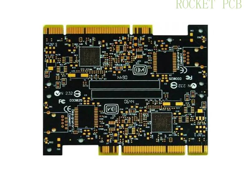
Gold Finger PCBs, or Gold Edge Connectors, are designed with a strip of gold plating along the board's edge, typically on one or more sides. These gold-plated contacts serve as the interface for connecting external components or devices, such as memory modules, expansion cards, or connectors, to the PCB.
The gold plating provides several advantages, making Gold Finger PCBs the preferred choice for critical applications. Gold is highly conductive and corrosion-resistant, offering excellent signal integrity and prolonged service life. Moreover, its softness allows for effective mating and demating, making it ideal for repeated connection cycles.
Gold Finger PCBs are commonly found in mission-critical devices where reliable and uninterrupted electrical connections are paramount. These applications include data centers, telecommunications infrastructure, military equipment, and medical devices.
While gold is known for its exceptional properties, it is only partially immune to specific challenges. Gold diffusion is one of the primary concerns in Gold Finger PCBs, where gold atoms migrate into neighboring materials over TimeTime. This diffusion can compromise the integrity of the gold plating, leading to diminished electrical conductivity and potential signal degradation.
Another critical issue is gold embrittlement, which occurs when gold atoms penetrate the base materials of the PCB, making them more brittle and prone to fractures under mechanical stress. Gold embrittlement can lead to the development of micro-cracks or complete failure of the PCB's connections, jeopardizing the reliability of the entire system.
This article aims to provide valuable insights and practical strategies for engineers and potential buyers of Gold Finger PCBs. By understanding the challenges associated with gold diffusion and embrittlement, engineers can make informed decisions during the design and manufacturing process to ensure the long-term reliability of their products.
II.Understanding Gold Diffusion and Embrittlement in Gold Finger PCBs
A.Explanation of Gold Diffusion and its Impact on PCB Performance
Gold diffusion is a phenomenon that occurs in Gold Finger PCBs over TimeTime, where gold atoms migrate into adjacent materials due to thermal or mechanical stress. This migration of gold atoms can adversely affect the performance and reliability of the PCB.
Factors Influencing Gold Diffusion
Several factors contribute to gold diffusion in Gold Finger PCBs:
1. Temperature: High temperatures experienced during PCB assembly and reflow processes can accelerate gold diffusion. The elevated temperatures cause the gold atoms to diffuse into nearby materials, changing the gold plating's integrity.
2. Contamination: The presence of contaminants, such as sulfur or oxygen, can promote gold diffusion by forming compounds with gold atoms that are more mobile and prone to distribution.
3. Mechanical Stress: Mechanical stress during PCB operation or assembly can induce gold diffusion by creating vacancies in the crystal lattice structure, facilitating the movement of gold atoms.
Effects of Gold Diffusion
Gold diffusion can have several detrimental effects on Gold Finger PCBs:
1. Increased Electrical Resistance: Gold diffusion reduces the purity of the gold plating, leading to higher electrical resistance in the gold traces. This increased resistance can result in signal degradation and loss.
2. Corrosion Susceptibility: Gold diffusion can compromise the protective properties of gold plating, making the PCB more susceptible to corrosion from external elements.
3. Intermetallic Formation: Diffused gold atoms can react with other metals in the PCB, forming intermetallic compounds that weaken the PCB's structure and connections.
B.The Concept of Gold Embrittlement and Its Consequences on PCB Reliability
Gold embrittlement is a related concern in Gold Finger PCBs, where gold atoms diffuse into the base materials of the PCB, making them more brittle. This phenomenon can lead to mechanical failures and reduced reliability of the PCB.
Causes of Gold Embrittlement
Gold embrittlement is primarily caused by the diffusion of gold atoms into the underlying metals, such as copper, in the PCB. This diffusion can occur during PCB assembly processes, especially soldering or reflow.
Effects of Gold Embrittlement
Gold embrittlement can have severe consequences on the reliability of Gold Finger PCBs:
1. Micro-Cracks Formation: Gold embrittlement can create micro-cracks in the PCB's base materials, leading to intermittent connections or complete failures.
2. Reduced Mechanical Durability: The embrittled base materials are more susceptible to mechanical stress, making the PCB vulnerable to damage during handling or operation.
3. Weakened Solder Joints: Gold embrittlement can weaken solder joints, leading to fractures and subsequent disconnection of components.
Understanding gold diffusion and embrittlement is crucial in ensuring the long-term reliability of Gold Finger PCBs. Engineers and manufacturers must be vigilant in mitigating these effects through appropriate design, material selection, and process controls during PCB manufacturing. By addressing gold diffusion and embrittlement concerns, Gold Finger PCB service providers, including those in China, can offer high-quality and reliable products to meet the demanding requirements of various industries. Proper testing and qualification can further enhance the overall performance and durability of Gold Finger PCBs, assuring customers of their lasting functionality and value.
III.Factors Contributing to Gold Diffusion and Embrittlement
Various factors influence gold diffusion and embrittlement in Gold Finger PCBs during the PCB manufacturing and assembly processes. Understanding these contributing factors is essential for implementing effective mitigation strategies to ensure the long-term reliability of PCBs.
A.Impact of High Temperatures during PCB Assembly and Reflow Processes
One of the primary contributors to gold diffusion and embrittlement in Gold Finger PCBs is exposure to high temperatures during the assembly and reflow processes. These elevated temperatures can promote the migration of gold atoms, compromising the integrity of the gold plating and the PCB.
1. Soldering and Reflow Processes
During PCB assembly, soldering and reflow processes involve subjecting the PCBs to elevated temperatures to facilitate the bonding of components. These high temperatures can lead to the diffusion of gold atoms into adjacent materials, such as copper traces and solder joints.
2. Thermal Cycling
Thermal cycling can exacerbate gold diffusion in applications where Gold Finger PCBs are exposed to temperature variations, such as automotive or aerospace industries. Repeated temperature changes cause the expansion and contraction of materials, creating microstructural defects that encourage the migration of gold atoms.
3. Reflow Profiles
The specific reflow profiles used during PCB assembly play a critical role in determining the extent of gold diffusion. Rapid temperature changes or prolonged exposure to high temperatures can accelerate diffusion, increasing embrittlement risks.
B.Influence of Contamination and Impurities on Gold Plating
Contamination and impurities in the PCB manufacturing process can also contribute to gold diffusion and embrittlement. Unwanted substances can react with gold atoms, forming compounds that are more susceptible to distribution.
1. Presence of Sulfur and Oxygen
Sulfur and oxygen are common contaminants found in PCB manufacturing environments. These elements can react with gold atoms, creating sulfides and oxides that facilitate gold diffusion. Controlling the level of sulfur and oxygen is crucial to prevent such reactions.
2. Surface Finish and Plating Quality
The quality of the gold plating and surface finish significantly impacts the diffusion and embrittlement tendencies of Gold Finger PCBs. Proper plating techniques, such as Electroless Nickel Immersion Gold (ENIG), can offer enhanced protection against diffusion, reducing the risks of embrittlement.
3. Contaminants from Handling and Storage
Contaminants introduced while handling and storing Gold Finger PCBs can also play a role in gold diffusion. Proper handling procedures and storage conditions should be maintained to prevent exposure to harmful substances.
Various factors contribute to gold diffusion and embrittlement in Gold Finger PCBs. Understanding the impact of high temperatures during assembly and reflow processes and the influence of contamination and impurities is crucial for engineers and manufacturers to develop effective mitigation strategies. By carefully controlling the manufacturing processes and adopting suitable surface finishes, Gold Finger PCB suppliers can deliver reliable and durable products to meet the demands of diverse industries. Implementing measures to minimize gold diffusion and embrittlement ensures the long-term performance and reliability of Gold Finger PCBs, establishing them as a preferred choice for critical applications.
IV.Preventive Measures for Mitigating Gold Diffusion and Embrittlement in Gold Finger PCBs
To ensure the long-term reliability and performance of Gold Finger PCBs, engineers, and manufacturers can implement various preventive measures that address the challenges of gold diffusion and embrittlement. By adopting these measures, Gold Finger PCB service providers and suppliers can offer high-quality and dependable products tailored to the specific needs of diverse applications.
A.Selecting Appropriate Gold Thickness and Purity for Specific Applications
One of the first steps in mitigating gold diffusion and embrittlement is to carefully select the appropriate gold thickness and purity for the specific application of the Gold Finger PCB.
1. Gold Thickness
The thickness of the gold plating directly impacts its resistance to diffusion. For applications that require frequent mating and demating cycles, a thicker gold plating is advisable to withstand wear and tear without compromising the integrity of the gold layer.
2. Gold Purity
Higher gold purity is preferred to minimize the likelihood of diffusion. Gold with higher purity is less susceptible to reacting with contaminants and adjacent materials, reducing the potential for distribution.
B.Optimizing PCB Design and Layout to Minimize Stress on Gold-Plated Areas
Optimizing the PCB design and layout to minimize stress on gold-plated areas is essential to preventing gold diffusion and embrittlement.
1. Trace Routing
Engineers should carefully route traces during PCB layout design to avoid sharp bends or acute angles that could induce mechanical stress on the gold-plated areas. A well-designed trace layout ensures reduced pressure during temperature fluctuations or automatic loading.
2. Pad and Via Placement
Proper placement of pads and vias is essential to prevent stress concentration on gold-plated areas. Distributing the connection points evenly and ensuring adequate spacing can reduce the risk of embrittlement caused by localized stress.
3. Gold-to-Substrate Bonding
Implementing appropriate bonding techniques between the gold plating and the substrate material can enhance the overall mechanical robustness of the Gold Finger PCB. A strong and reliable bond minimizes the risk of gold detachment during operation.
C.Implementing Controlled Reflow Profiles during Assembly to Avoid Excessive Heat Exposure
Controlling the reflow profiles during PCB assembly is vital to prevent excessive heat exposure, which can accelerate gold diffusion and embrittlement.
1. Temperature Ramp Rates
Slower temperature ramp rates during the reflow process help minimize thermal shock and stress on the gold plating. Gradual heating and cooling reduce the chances of gold diffusion and subsequent embrittlement.
2. Peak Reflow Temperature
The peak reflow temperature should be carefully controlled to avoid reaching temperatures encouraging rapid gold diffusion. Staying within the recommended temperature limits ensures the integrity of the gold plating.
3. Dwell TimeTime
Controlling the dwell time, the duration the PCB spends at the peak reflow temperature, is critical in preventing prolonged exposure to high temperatures, which could lead to increased gold diffusion.
By implementing these preventive measures, engineers and Gold Finger PCB manufacturers can significantly reduce the risks of gold diffusion and embrittlement. Careful selection of gold thickness and purity, optimized PCB design and layout, and controlled reflow profiles during assembly play critical roles in ensuring the long-term reliability and performance of Gold Finger PCBs. Adopting these measures demonstrates a commitment to providing high-quality and dependable Gold Finger PCBs for a wide range of critical applications, solidifying the reputation of Gold Finger PCB suppliers' reputation as trusted electronics industry partners.
V.Gold Plating Process and Quality Control in Gold Finger PCBs
The gold plating process and subsequent quality control are critical to producing reliable and high-performance Gold Finger PCBs. To ensure the integrity and longevity of the gold plating, reputable and experienced PCB manufacturers follow stringent processes and utilize non-destructive testing methods.
A.Importance of Using Reputable and Experienced PCB Manufacturers
Selecting a reputable and experienced PCB manufacturer is paramount in achieving high-quality Gold Finger PCBs. A trusted manufacturer possesses the expertise, state-of-the-art equipment, and robust quality control systems to execute the gold plating process precisely and consistently.
1. Expertise in Gold Plating
Reputable manufacturers deeply understand gold plating techniques and their application in Gold Finger PCBs. Their expertise allows them to tailor the plating process to specific applications, ensuring optimal gold thickness and purity for improved resistance to diffusion and embrittlement.
2. Process Optimization
Experienced manufacturers continually refine their gold plating processes to maximize efficiency and minimize the risk of defects. Through careful process optimization, they can achieve uniform gold distribution and adhesion, enhancing the overall reliability of Gold Finger PCBs.
B.Ensuring Compliance with Industry Standards for Gold Plating Thickness and Quality
Adhering to industry standards for gold plating thickness and quality is crucial to maintain consistency and reliability in Gold Finger PCBs.
1.IPC-4552 Standard
The IPC-4552 standard defines the requirements for electroless nickel and immersion gold (ENIG) coatings commonly used in Gold Finger PCBs. Following this standard ensures that the gold plating thickness and composition meet industry-accepted guidelines for optimal performance.
2. Quality Assurance Measures
Reputable manufacturers implement robust quality assurance measures to monitor the gold plating process and ensure compliance with industry standards. Regular inspections, sample testing, and documentation are performed to guarantee consistent plating thickness and quality.
C.Non-Destructive Testing Methods to Assess Gold Plating Integrity
Non-destructive testing methods are employed to assess the integrity of the gold plating without damaging the PCB.
1. X-ray Fluorescence (XRF) Testing
XRF testing is commonly used to measure the thickness of the gold plating without physically altering the PCB. This non-destructive technique provides valuable data on the plating thickness and composition, helping manufacturers validate compliance with industry standards.
2. Scanning Electron Microscopy (SEM)
SEM enables detailed inspection of the gold plating surface at a microscopic level. By analyzing SEM images, manufacturers can identify potential defects, such as voids or discontinuities, and take corrective actions to ensure the quality of the gold plating.
The gold plating process and quality control measures are crucial in producing reliable and durable Gold Finger PCBs. Engaging reputable and experienced PCB manufacturers ensures the application of precise plating techniques, adherence to industry standards, and implementation of non-destructive testing methods. Gold Finger PCB suppliers can deliver products that meet various industries' stringent demands, earning customers' trust and satisfaction worldwide by focusing on process optimization and quality assurance. The commitment to excellence in gold plating and quality control establishes Gold Finger PCB manufacturers as valued partners in the electronics industry, supporting innovation and reliability in modern electronic devices and applications.
VI.Reliability Testing and Qualification for Gold Finger PCBs
Reliability testing and qualification are essential stages in ensuring the robustness and performance of Gold Finger PCBs under various operating conditions. Through rigorous testing, engineers and manufacturers can identify potential weaknesses, validate design choices, and demonstrate the long-term reliability of these critical electronic components.
A.Accelerated Life Testing to Evaluate PCB Performance under Harsh Conditions
Accelerated life testing involves subjecting Gold Finger PCBs to accelerated stress conditions that simulate the effects of extended usage over TimeTime. This testing compresses the product's lifespan into a shorter duration, allowing engineers to assess its reliability under harsh conditions.
1. Purpose of Accelerated Life Testing
Accelerated life testing serves several purposes, including:
· Predictive Reliability: It predicts the PCB's behavior and performance over its intended service life, allowing engineers to make informed decisions about design improvements.
· Product Validation: It validates the design and manufacturing processes, ensuring that the Gold Finger PCB can withstand the intended operating conditions.
2. Types of Accelerated Life Testing
a. High-Temperature Testing: Subjecting the PCB to elevated temperatures to evaluate its performance under thermal stress and identify potential issues such as gold diffusion and embrittlement.
b. Temperature Cycling: Cycling the PCB between high and low temperatures to assess its ability to withstand thermal expansion and contraction without compromising the gold plating.
B.Temperature Cycling and Thermal Shock Tests to Simulate Real-World Scenarios
Temperature cycling and thermal shock tests simulate real-world scenarios in which Gold Finger PCBs experience temperature fluctuations due to environmental changes or operational conditions.
1. Temperature Cycling
Temperature cycling involves subjecting the PCB to a series of temperature changes between high and low extremes. This test evaluates the PCB's resistance to thermal stresses, including any effects on the gold plating and solder joints.
2. Thermal Shock
Thermal shock tests expose the PCB to rapid temperature transitions, simulating sudden changes in environmental conditions. This test helps assess the impact of thermal shocks on the PCB's reliability, solder joint integrity, and resistance to gold diffusion.
C.Assessment of Gold Diffusion Resistance through Extended Reliability Testing
Extended reliability testing involves subjecting Gold Finger PCBs to continuous operation under normal conditions for an extended period. This comprehensive testing allows engineers to monitor the PCB's behavior over TimeTime, particularly concerning gold diffusion and embrittlement.
1. Long-Term Exposure
The extended reliability testing includes long-term exposure to temperature variations and mechanical stress that the PCB may experience during its operational life.
2. Detection of Anomalies
By continuously monitoring the PCB's performance during the extended testing period, engineers can detect any anomalies, such as changes in electrical properties or signs of gold diffusion, that may arise over TimeTime.
Reliability testing and qualification are crucial in ensuring the robustness and durability of Gold Finger PCBs. Accelerated life testing, temperature cycling, thermal shock tests, and extended reliability testing collectively validate the design choices, assess the performance under harsh conditions, and confirm the resistance to gold diffusion and embrittlement. By subjecting Gold Finger PCBs to rigorous testing and qualification processes, manufacturers can confidently deliver products that meet the highest standards of reliability and performance, reassuring customers of their long-term value and dependability in various critical applications.
VII.Failure Analysis and Detection for Gold Finger PCBs
Failure analysis and detection are crucial to maintaining the reliability and performance of Gold Finger PCBs in the field. When issues related to gold diffusion and embrittlement arise, thorough analysis and corrective actions are essential to prevent further occurrences and ensure the continued functionality of the PCBs.
A.Identifying Potential Signs of Gold Diffusion and Embrittlement in Fielded PCBs
Timely identification of potential signs of gold diffusion and embrittlement is vital for addressing issues before they escalate into critical failures. Engineers and technicians must be vigilant in monitoring fielded Gold Finger PCBs for any visible degradation indicators.
1. Visual Inspection
Regular visual inspections of Gold Finger PCBs can reveal signs of gold diffusion, such as discoloration, tarnishing, or uneven gold thickness. Physical observations of solder joints and gold-plated contacts can also help identify potential embrittlement-related issues, such as micro-cracks or fractured connections.
2. Electrical Testing
Conducting electrical testing and measuring signal integrity in fielded Gold Finger PCBs can provide insight into potential gold diffusion effects on the PCB's electrical performance. Increased electrical resistance or intermittent connectivity can indicate the presence of gold diffusion and embrittlement-related concerns.
B.Analyzing Failure Modes and Root Causes Using Advanced Techniques
In the event of PCB failures related to gold diffusion or embrittlement, in-depth analysis using advanced techniques is necessary to identify the root causes and implement practical corrective actions.
1. Microsectioning
Microsectioning involves cutting and examining a cross-section of the PCB under a microscope. This technique allows engineers to investigate the condition of the gold plating and the integrity of the interface between the gold and substrate materials. Microsectioning can reveal embrittlement-related issues and diffusion effects on the gold plating.
2. Scanning Electron Microscopy (SEM)
SEM analysis provides detailed images of the PCB's surface and microstructures. Using SEM, engineers can visualize the extent of gold diffusion, intermetallic formations, and other structural anomalies contributing to the failure.
3. Energy-Dispersive X-ray Spectroscopy (EDS)
EDS is employed in conjunction with SEM to analyze the elemental composition of specific areas on the PCB. It helps identify any impurities or contaminants that might have contributed to gold diffusion or embrittlement.
C.Implementing Corrective Actions to Prevent Future Occurrences
Based on the findings from failure analysis, engineers can implement targeted corrective actions to prevent similar issues in future Gold Finger PCBs.
1. Process Improvements
Identifying and addressing process deficiencies in gold plating and PCB manufacturing can significantly reduce the risk of gold diffusion and embrittlement. This may involve adjusting temperature profiles during assembly, refining plating techniques, or optimizing surface finish choices.
2. Material Enhancements
Selecting materials with improved resistance to gold diffusion and embrittlement, such as more reliable substrates or alternative plating methods, can enhance the overall performance and longevity of Gold Finger PCBs.
3. Design Modifications
Making design modifications, such as adjusting trace widths or pad layouts, can reduce stress on gold-plated areas and enhance the overall mechanical durability of the PCB.
Failure analysis and detection are integral components of maintaining the reliability and performance of Gold Finger PCBs. By identifying potential signs of gold diffusion and embrittlement in fielded PCBs and analyzing failure modes using advanced techniques, engineers can implement targeted corrective actions to prevent future occurrences. Through continuous improvement and adherence to best practices, Gold Finger PCB manufacturers and service providers can offer products that meet the highest standards of quality and reliability, ensuring the satisfaction and confidence of their customers in various critical applications.
VIII.Conclusion
Preventing gold diffusion and embrittlement in Gold Finger PCBs is paramount to ensure electronic devices' long-term reliability and performance. As a reputable brand in the industry, Rocket-PCB understands the critical role engineers and reliable manufacturing processes play in delivering high-quality Gold Finger PCBs.
Gold diffusion, the migration of gold atoms into adjacent materials, can degrade the electrical conductivity and compromise the functionality of the PCB. Simultaneously, gold embrittlement can lead to mechanical failures and reduced overall reliability.
Rocket-PCB emphasizes the significance of selecting appropriate gold thickness and purity for specific applications, optimizing PCB designs to minimize stress on gold-plated areas, and implementing controlled reflow profiles during assembly.
These measures effectively mitigate the risks of gold diffusion and embrittlement, ensuring that the Gold Finger PCBs meet the stringent requirements of various industries.
Rocket-PCB's commitment to excellence extends to its adherence to industry standards for gold plating thickness and quality. With state-of-the-art equipment and robust quality control systems, Rocket-PCB ensures consistency and reliability in every batch of Gold Finger PCBs.
Furthermore, reliability testing and qualification are integral parts of Rocket-PCB's approach to delivering high-quality products. Accelerated life testing, temperature cycling, thermal shock tests, and extended reliability testing validate the PCB's ability to withstand harsh conditions and resist gold diffusion and embrittlement.
Rocket-PCB's dedicated team conducts timely failure analysis and detection in the field to identify any potential signs of gold diffusion or embrittlement. Advanced techniques such as microsectioning, scanning electron microscopy (SEM), and energy-dispersive X-ray spectroscopy (EDS) enable precise root cause analysis and the implementation of targeted corrective actions.
Rocket-PCB's success stories include numerous case studies and real-world examples of Gold Finger PCB implementations that have surpassed industry standards and customer expectations. Rocket-PCB's Gold Finger PCBs have consistently demonstrated exceptional performance and reliability, from critical applications in data centers and automotive electronics to medical devices and telecommunications equipment.
Rocket-PCB's focus on prevention, thorough testing, and continuous improvement cements its position as a trusted and reliable brand in the electronics industry. By prioritizing quality and innovation, Rocket-PCB continues to contribute to technological advancements and support the success of electronic devices worldwide.


